What is PCB Manufacturing?
PCB manufacturing is the process of creating printed circuit boards (PCBs) that are used in various electronic devices. PCBs are essential components in modern electronics, providing a platform for electrical components to be mounted and connected. The manufacturing process involves several steps, including design, fabrication, assembly, and testing.
The Importance of PCB Manufacturing
PCBs are crucial in the electronics industry for several reasons:
- They provide a compact and efficient way to connect electronic components.
- PCBs allow for the miniaturization of electronic devices.
- They ensure reliable and consistent performance of electronic circuits.
- PCBs enable mass production of electronic devices, reducing costs and increasing efficiency.
The PCB Manufacturing Process
The PCB manufacturing process consists of several stages, each requiring specific expertise and technology. The main stages include:
1. PCB Design
The first step in PCB manufacturing is the design phase. This involves creating a schematic diagram of the electronic circuit and then converting it into a PCB layout. The layout determines the positioning of components, traces, and vias on the board.
PCB Design Software
Several software tools are used for PCB design, including:
- Altium Designer
- Eagle PCB
- KiCad
- OrCAD
- Mentor Graphics PADS
These tools allow designers to create complex PCB layouts, simulate circuit behavior, and generate manufacturing files.
2. PCB Fabrication
Once the PCB design is complete, the next stage is fabrication. This involves creating the physical PCB based on the design files. The fabrication process includes several sub-stages:
a. Printing the Circuit Pattern
The first step in PCB fabrication is to print the circuit pattern onto a copper-clad laminate. This is typically done using a photoresist coating and exposure to UV light. The exposed areas of the photoresist are then developed and removed, leaving the desired circuit pattern.
b. Etching
After the circuit pattern is printed, the unwanted copper is removed through an etching process. This involves immersing the PCB in an etchant solution, which chemically removes the exposed copper, leaving only the desired circuit traces.
c. Drilling
Once the etching is complete, holes are drilled into the PCB to accommodate through-hole components and vias. This is done using specialized drilling machines that can create holes of various sizes with high precision.
d. Plating
After drilling, the holes are plated with a conductive material, usually copper, to ensure proper electrical connection between layers. This is followed by a final plating process, which typically involves applying a layer of tin-lead or other protective coatings to the copper traces.
e. Solder Mask and Silkscreen
The final step in PCB fabrication is the application of a solder mask and silkscreen. The solder mask is a protective coating that covers the copper traces, leaving only the areas intended for soldering exposed. The silkscreen is a printed layer that adds text, logos, and other identifying marks to the PCB.
3. PCB Assembly
After the PCB is fabricated, the next stage is assembly. This involves mounting and soldering electronic components onto the board. PCB assembly can be done manually or using automated machines.
a. Surface Mount Technology (SMT)
SMT is a method of mounting components directly onto the surface of the PCB. This is done using a pick-and-place machine, which accurately places components onto the board, followed by a reflow soldering process that melts the solder paste and secures the components in place.
b. Through-Hole Technology (THT)
THT involves inserting component leads through holes in the PCB and soldering them on the opposite side. This method is less common in modern PCBs but is still used for certain components that require greater mechanical stability.
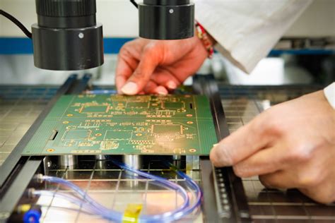
4. PCB Testing
The final stage in PCB manufacturing is testing. This involves verifying that the assembled PCB functions as intended and meets the required specifications. Several types of tests can be performed, including:
- Visual inspection
- Automated Optical Inspection (AOI)
- In-Circuit Testing (ICT)
- Functional Testing
These tests help identify any manufacturing defects, component failures, or design issues, ensuring that the final product is of high quality and reliability.

PCB Manufacturing Standards and Certifications
To ensure consistent quality and reliability, PCB manufacturing adheres to various industry standards and certifications. Some of the most common standards include:
- IPC (Association Connecting Electronics Industries) Standards:
- IPC-A-600: Acceptability of Printed Boards
- IPC-A-610: Acceptability of Electronic Assemblies
- IPC-6012: Qualification and Performance Specification for Rigid Printed Boards
- UL (Underwriters Laboratories) Standards:
- UL 94: Standard for Safety of Flammability of Plastic Materials
- UL 796: Standard for Safety of Printed-Wiring Boards
- RoHS (Restriction of Hazardous Substances) Directive
- REACH (Registration, Evaluation, Authorization, and Restriction of Chemicals) Regulation
Adhering to these standards ensures that PCBs are manufactured using safe materials and processes, and meet the required performance and reliability criteria.

Advances in PCB Manufacturing
PCB manufacturing technology continues to evolve, driven by the demand for smaller, faster, and more complex electronic devices. Some of the recent advances in PCB manufacturing include:
1. High-Density Interconnect (HDI) PCBs
HDI PCBs feature finer traces, smaller vias, and higher component density than traditional PCBs. This enables the creation of more compact and high-performance electronic devices.
2. Flexible and Rigid-flex PCBs
Flexible PCBs are made from flexible substrate materials, allowing them to bend and conform to various shapes. Rigid-flex PCBs combine rigid and flexible sections, providing both mechanical stability and flexibility where needed.
3. Embedded Components
Embedded components are electronic components that are integrated into the inner layers of a PCB, rather than being mounted on the surface. This technique saves space and improves signal integrity, enabling the creation of more compact and high-performance devices.
4. 3D Printing
3D printing technology is being explored for PCB manufacturing, potentially enabling the creation of complex, three-dimensional circuit structures and reducing the time and cost of prototyping.

FAQ
-
Q: What is the difference between a single-layer and multi-layer PCB?
A: A Single-Layer PCB has all components and traces on one side of the board, while a multi-layer PCB has multiple layers of traces and components sandwiched between insulating layers. Multi-layer PCBs offer higher component density and better signal integrity. -
Q: What is the purpose of a solder mask on a PCB?
A: A solder mask is a protective coating applied to the copper traces of a PCB, leaving only the areas intended for soldering exposed. It prevents accidental short circuits and protects the traces from oxidation and damage. -
Q: What is the difference between SMT and THT assembly?
A: SMT (Surface Mount Technology) involves mounting components directly onto the surface of the PCB, while THT (Through-Hole Technology) involves inserting component leads through holes in the PCB and soldering them on the opposite side. SMT is more common in modern PCBs due to its higher component density and faster assembly process. -
Q: What is the purpose of testing in PCB manufacturing?
A: Testing in PCB manufacturing is conducted to verify that the assembled PCB functions as intended and meets the required specifications. It helps identify any manufacturing defects, component failures, or design issues, ensuring that the final product is of high quality and reliability. -
Q: What are some of the industry standards that PCB manufacturing adheres to?
A: PCB manufacturing adheres to various industry standards to ensure consistent quality and reliability. Some of the most common standards include IPC (Association Connecting Electronics Industries) standards, UL (Underwriters Laboratories) standards, RoHS (Restriction of Hazardous Substances) Directive, and REACH (Registration, Evaluation, Authorization, and Restriction of Chemicals) Regulation.
Conclusion
PCB manufacturing is a complex and multi-stage process that plays a crucial role in the production of modern electronic devices. From design to fabrication, assembly, and testing, each stage requires specific expertise and technology to ensure the creation of high-quality and reliable PCBs.
As electronic devices continue to become smaller, faster, and more complex, PCB manufacturing technology must evolve to keep pace. Advances such as HDI PCBs, flexible and rigid-flex PCBs, embedded components, and 3D printing are shaping the future of PCB manufacturing and enabling the creation of innovative electronic products.
By understanding the fundamentals of PCB manufacturing and staying informed about the latest industry trends and standards, engineers and manufacturers can ensure that they are producing PCBs that meet the highest standards of quality, reliability, and performance.
No responses yet