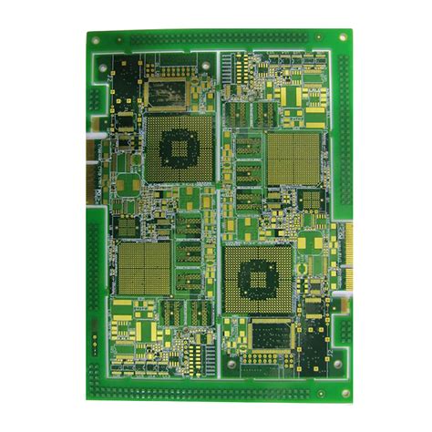
What is an HDI PCB?
An HDI PCB is a printed circuit board that features higher wiring density per unit area compared to conventional PCBs. This is achieved through the use of smaller vias, finer traces, and advanced manufacturing techniques. HDI PCBs enable the miniaturization of electronic devices while maintaining or improving their functionality and performance.
Advantages of HDI PCBs
- Reduced size and weight
- Improved signal integrity
- Higher component density
- Enhanced thermal management
- Increased reliability
HDI PCB Design Considerations
When designing an HDI PCB, several key factors must be taken into account to ensure optimal performance and manufacturability.
Component Selection and Placement
Choosing the right components and placing them strategically on the PCB is crucial for HDI designs. Consider the following:
- Use small-footprint components, such as chip-scale packages (CSPs) and ball grid arrays (BGAs)
- Place components on both sides of the board to maximize space utilization
- Group related components together to minimize trace lengths and improve signal integrity
Signal Integrity and EMI Reduction
Maintaining signal integrity and minimizing electromagnetic interference (EMI) are critical in HDI PCB design. Implement the following techniques:
- Use controlled impedance traces to match the impedance of the source and load
- Employ proper grounding techniques, such as ground planes and stitching vias
- Incorporate EMI shielding measures, like copper pours and shielding cans
Thermal Management
HDI PCBs often have higher power densities, making thermal management a key concern. Consider the following strategies:
- Use thermal vias to transfer heat from components to the opposite side of the board
- Incorporate copper pours and heat spreaders to dissipate heat evenly
- Select materials with appropriate thermal conductivity, such as metal-core substrates

HDI PCB Manufacturing Processes
The manufacturing of HDI PCBs involves several advanced techniques and processes to achieve the required high density and precision.
Via Formation
HDI PCBs employ various types of vias, including:
- Microvias: Laser-drilled vias with diameters less than 150µm
- Buried vias: Vias that connect inner layers but do not extend to the outer layers
- Blind vias: Vias that start from an outer layer and terminate at an inner layer
Lamination and Pressing
The lamination and pressing process for HDI PCBs requires precise control to ensure proper bonding and minimize warpage. Key considerations include:
- Using low-flow prepregs and core materials to reduce resin flow and maintain via integrity
- Employing multiple lamination cycles for complex multilayer stackups
- Controlling the pressing temperature and pressure to minimize thermal stress
Surface Finish and Solder Mask Application
The surface finish and solder mask application are critical for HDI PCBs to ensure reliable soldering and protection. Common options include:
- Immersion gold (ENIG) for its flatness and durability
- Electroless nickel electroless palladium immersion gold (ENEPIG) for improved solder joint reliability
- Liquid photoimageable (LPI) solder mask for high resolution and fine pitch applications

Best Practices for Achieving a Perfect HDI PCB
To achieve a perfect HDI PCB, follow these best practices:
- Collaborate closely with your PCB manufacturer throughout the design and fabrication process
- Use design for manufacturability (DFM) guidelines to ensure your design is compatible with the chosen manufacturing processes
- Perform thorough design rule checks (DRC) and layout vs. schematic (LVS) checks to identify and resolve any errors or violations
- Conduct signal integrity simulations to verify the performance of critical signals and optimize the design accordingly
- Implement a comprehensive testing and inspection plan to validate the functionality and reliability of the manufactured HDI PCBs

Frequently Asked Questions (FAQ)
1. What is the minimum via size achievable in HDI PCBs?
The minimum via size in HDI PCBs depends on the specific manufacturing capabilities of the PCB fabricator. Typically, microvias can have diameters as small as 50-100µm, while buried and blind vias may have slightly larger minimum sizes.
2. How many layers can an HDI PCB have?
HDI PCBs can have varying numbers of layers depending on the design requirements and manufacturing capabilities. Common layer counts for HDI PCBs range from 4 to 16 layers, but some advanced designs may have even more layers.
3. What is the typical turnaround time for HDI PCB fabrication?
The turnaround time for HDI PCB fabrication varies depending on the complexity of the design, the chosen manufacturer, and the manufacturing processes involved. Generally, HDI PCBs have longer lead times compared to standard PCBs, ranging from 2-5 weeks or more.
4. How do I choose the right surface finish for my HDI PCB?
The choice of surface finish for an HDI PCB depends on factors such as the intended application, soldering requirements, shelf life, and cost. ENIG and ENEPIG are popular choices for their reliability and compatibility with fine-pitch components, while OSP (Organic Solderability Preservative) may be suitable for less demanding applications.
5. Are there any specific design tools for HDI PCBs?
Most modern PCB design software, such as Altium Designer, Cadence Allegro, and Mentor Graphics PADS, have features and capabilities specifically tailored for HDI PCB design. These tools offer advanced routing, via placement, and signal integrity analysis functionalities to facilitate the design process.
| HDI PCB Layer Count | Typical Applications |
|---|---|
| 4-6 layers | Smartphones, wearables, IoT devices |
| 8-10 layers | Tablets, laptops, advanced medical devices |
| 12-16 layers | High-performance computing, aerospace, and defense |
In conclusion, achieving a perfect HDI PCB requires careful consideration of design factors, manufacturing processes, and best practices. By understanding the intricacies of HDI PCB technology and collaborating closely with experienced PCB manufacturers, you can unlock the full potential of HDI PCBs in your electronic devices and stay ahead of the curve in this rapidly evolving industry.
No responses yet