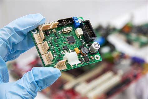
What is Fine Pitch PCB Assembly?
Fine Pitch PCB assembly refers to the process of assembling electronic components onto a printed circuit board (PCB) with a very small distance between the leads or pins of the components. Typically, a pitch of 0.5mm or less is considered “fine pitch.”
Fine pitch PCB assembly allows for the creation of smaller, more compact electronic devices. As consumer demand for ever-shrinking gadgets continues to grow, manufacturers are turning to fine pitch PCB assembly to pack more functionality into less space.
Benefits of Fine Pitch PCB Assembly
- Enables smaller, lighter, thinner devices
- Allows for higher component density
- Improves electrical performance
- Reduces material costs
However, fine pitch PCB assembly also presents some challenges compared to standard PCB assembly:
- Requires specialized equipment and processes
- Components are more fragile and prone to damage
- Inspection and rework is more difficult
- Higher defect rates are common
0.5mm – The Frontier of Fine Pitch
While 0.5mm pitch components were once considered leading-edge, they are now relatively mainstream in PCB assembly. Most Tier 1 and Tier 2 EMS providers are capable of routinely assembling 0.5mm pitch components with high yields.
Common 0.5mm pitch packages include:
| Package | Pin Count | Size (mm) |
|---|---|---|
| QFP | Up to 256 | 28 x 28 |
| QFN | Up to 132 | 10 x 10 |
| BGA | Up to 324 | 15 x 15 |
As 0.5mm has become the new standard, manufacturers are pushing the boundaries to even finer pitches in order to enable the next generation of miniaturized products. 0.4mm, 0.3mm and below are now the frontier of fine pitch PCB assembly.

Breaking the 0.3mm Barrier
Assembling PCBs with 0.3mm pitch components requires extremely precise processes and specialized equipment beyond the capability of most assembly shops. Placement machines need to have exceptional accuracy, and soldering processes must be tightly controlled to prevent bridging and tombstoning defects.
Some of the challenges of 0.3mm and finer pitch assembly include:
- Fragile leads prone to bending and damage
- Tighter placement tolerances required
- Precise paste deposition and volume control critical
- Reflow soldering window very narrow
- Extensive inspection required, rework difficult
Despite the difficulties, 0.3mm pitch BGAs and CSPs are increasingly being used in advanced applications such as:
- Mobile processors
- High-bandwidth memory
- RF transceivers
- Cryptoprocessors
Companies like Apple and Samsung are driving the adoption of ultra-fine pitch packaging as they push for thinner, more powerful smartphones and wearables. As 0.3mm solutions become more widespread, leading assembly providers are already looking ahead to the next milestone.

The Ultimate Challenge: 0.05mm Assembly
For most people, it’s hard to even imagine components and PCBs with features as small as 50 microns (0.05mm). This is truly at the limits of conventional PCB fabrication and assembly technology. However, some cutting-edge research has demonstrated the feasibility of 0.05mm interconnects.
In 2019, scientists at Taiwan’s Industrial Technology Research Institute (ITRI) successfully fabricated and assembled a test chip with 0.05mm pitch copper pillar bumps. The demonstration required state-of-the-art processes including:
- Semi-additive patterning (SAP) of superfine circuits
- Precise laser drilling of microvias
- Electroless nickel/palladium/gold (ENEPIG) surface finish
- High-resolution solder paste printing
- Chip-to-wafer stacking and bonding
While 0.05mm assembly is still firmly in the research phase, it points the way to the future of semiconductor packaging and integration. As Moore’s Law slows down, advanced packaging technologies will be key to enabling continued improvements in electronic device density and performance.
Roadmap to 0.05mm and Beyond
The journey to ultra-fine pitch assembly requires overcoming significant technical hurdles at every stage of the PCB Development process:
| Process | Current Capability | Roadmap |
|---|---|---|
| PCB Traces | 30-50μm width | 10-20μm |
| Microvias | 50-100μm diameter | 10-20μm |
| Solder Paste | 100-150μm dots | 20-50μm |
| Placement | ±25μm accuracy | ±5μm |
| Inspection | 10-20μm resolution | <5μm |
Closing these technology gaps will require sustained investment in R&D and collaboration across the electronics manufacturing supply chain. But if history is any guide, the relentless drive towards miniaturization will continue to push the limits of PCB design and assembly capabilities.

Partnering for Success in Fine Pitch PCBA
For most OEMs and product designers, fine pitch PCB assembly is not a core competency. Attempting to set up an in-house assembly line for leading-edge pitches is often impractical and cost-prohibitive.
Partnering with an experienced EMS provider is usually the best approach when you need fine pitch PCBA for your products. The right assembly partner will have:
- Modern equipment installed and qualified for fine pitch
- Robust processes with proven high yields
- Experienced engineers who understand fine pitch challenges
- Flexibility to customize specifications and requirements
- Commitment to quality and continuous improvement
When evaluating potential fine pitch PCBA partners, be sure to ask detailed questions about their capabilities, quality metrics, and experience with your specific pitch and packaging requirements. Visiting the facility and meeting the team in person is also highly recommended.
Conclusion
The evolution of fine pitch PCB assembly has been a key enabler of the incredible advances in electronic devices we’ve witnessed over the past few decades. As pitches continue to shrink to 0.05mm and beyond, PCBA specialists will play a central role in turning the latest packaging innovations into real products.
While fine pitch assembly is not without its challenges, the benefits in terms of device performance, portability and functionality are clear. With the right design, process and partners, fine pitch PCBA is well within reach for most products today. As we look ahead to a 0.05mm future, fine pitch will only become more critical.
Frequently Asked Questions
What is considered fine pitch in PCB assembly?
In PCB assembly, a pitch of 0.5mm or less between component leads is typically considered “fine pitch.” Some common fine pitch components include 0.5mm, 0.4mm, 0.3mm and smaller BGAs, CSPs and QFNs.
Why is fine pitch PCBA used?
Fine pitch PCBA allows for smaller, thinner and lighter electronic products. By reducing the space between component leads, more functionality can be packed into compact form factors. Fine pitch also improves electrical performance in some cases.
Is fine pitch PCBA more expensive?
In general, yes, fine pitch PCBA has higher costs compared to standard assembly. The specialized equipment, materials and skills required all contribute to greater expense. However, the trend is towards more mainstream adoption of fine pitch, which should help moderate cost premiums over time.
What are the risks and challenges with fine pitch assembly?
Some key challenges in fine pitch PCBA include fragile components prone to damage, tighter assembly process windows, higher defect rates, difficulties with inspection and rework. Designing for manufacturability and thorough process control are critical to mitigating these risks.
How can I find a reliable fine pitch PCBA partner?
Look for an experienced EMS provider with modern equipment, robust fine pitch processes, and a strong quality track record. Ask for customer references, and consider visiting the facility to assess capabilities first-hand. Clearly communicate your specific requirements and expect some back-and-forth to dial in the optimal manufacturing strategy.
No responses yet