Introduction to PCB Inspection
Printed Circuit Board (PCB) assembly is a complex process that involves multiple stages, from design and fabrication to component placement and soldering. To ensure the quality and reliability of the final product, PCB inspection is a crucial step that cannot be overlooked. In this article, we will delve into the various aspects of the final inspection of PCB Assembly, including the types of inspections, techniques used, and best practices to follow.
What is PCB Inspection?
PCB inspection is the process of examining a printed circuit board to identify any defects, errors, or inconsistencies that may affect its functionality or reliability. This process is carried out at various stages of the PCB assembly process, but the final inspection is the most critical as it is the last opportunity to catch any issues before the board is shipped to the customer.
Why is PCB Inspection Important?
PCB inspection is essential for several reasons:
-
Quality Assurance: PCB inspection ensures that the final product meets the required quality standards and specifications, minimizing the risk of defects or failures in the field.
-
Cost Savings: Identifying and rectifying issues early in the manufacturing process can save significant costs associated with rework, repairs, or replacements later on.
-
Reputation Management: Delivering high-quality, reliable products helps maintain a good reputation and customer satisfaction, leading to repeat business and referrals.
Types of PCB Inspections
There are several types of PCB inspections that can be performed during the assembly process, each focusing on different aspects of the board. Some of the most common types of inspections include:
Visual Inspection
Visual inspection is the most basic and widely used method of PCB inspection. It involves a trained operator visually examining the board for any obvious defects, such as missing components, incorrect component placement, or solder bridging. This inspection can be performed with the naked eye or using magnification tools like microscopes or magnifying lamps.
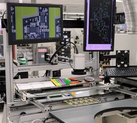
Automated Optical Inspection (AOI)
Automated Optical Inspection (AOI) is a computer-based inspection method that uses high-resolution cameras and advanced image processing algorithms to detect defects on the PCB. AOI systems can quickly scan the entire board and compare it to a predefined set of rules or a golden sample, identifying any discrepancies or anomalies.
X-Ray Inspection
X-ray inspection is used to examine the internal structure of the PCB, particularly for hidden or obscured components like Ball Grid Arrays (BGAs) or solder joints underneath components. This non-destructive technique allows operators to detect issues such as voids, cracks, or Insufficient Solder coverage that may not be visible from the surface.
In-Circuit Testing (ICT)
In-Circuit Testing (ICT) is a functional test that verifies the electrical connectivity and performance of individual components on the PCB. This test is performed using a bed-of-nails fixture that makes contact with specific test points on the board, allowing the system to measure resistance, capacitance, and other electrical properties.
Functional Testing
Functional testing is a comprehensive test that verifies the overall functionality and performance of the assembLED PCB. This test typically involves powering up the board and running a series of test routines to ensure that all components and subsystems are working as intended, and the board meets the specified requirements.

PCB Inspection Techniques
To effectively inspect PCBs, various techniques and tools are employed depending on the type of inspection and the specific requirements of the project. Some of the most common PCB inspection techniques include:
Manual Inspection
Manual inspection relies on the skill and experience of human operators to visually examine the PCB for defects. This technique is often used in conjunction with other inspection methods and is particularly useful for identifying issues that may not be easily detectable by automated systems, such as Component Orientation or labeling errors.
Automated Inspection
Automated inspection systems, such as AOI and X-ray machines, use advanced technology to scan the PCB and detect defects quickly and accurately. These systems can be programmed with specific rules and tolerances, allowing them to identify a wide range of issues, from missing components to solder defects.
Comparison Inspection
Comparison inspection involves comparing the assembled PCB to a known good reference, such as a golden sample or CAD data. This technique is useful for detecting any deviations from the intended design, such as incorrect component placement or routing errors.
Electrical Testing
Electrical testing techniques, like ICT and functional testing, are used to verify the electrical performance and functionality of the assembled PCB. These tests can help identify issues such as short circuits, open connections, or component failures that may not be visually apparent.

Best Practices for PCB Inspection
To ensure effective and efficient PCB inspection, consider the following best practices:
-
Establish Clear Inspection Criteria: Define clear and measurable inspection criteria based on the project requirements, industry standards, and customer specifications. This helps ensure consistency and accuracy in the inspection process.
-
Train and Certify Operators: Invest in training and certifying inspection operators to ensure they have the necessary skills and knowledge to perform their tasks effectively. Regular training updates can help keep operators current with the latest techniques and technologies.
-
Use Appropriate Inspection Equipment: Select inspection equipment that is suitable for the specific requirements of the project, considering factors such as board complexity, component types, and production volume. Regularly calibrate and maintain the equipment to ensure optimal performance.
-
Implement Statistical Process Control (SPC): Use SPC techniques to monitor and control the inspection process, identifying trends or anomalies that may indicate potential issues. This data-driven approach can help optimize the inspection process and reduce defects over time.
-
Document and Analyze Inspection Results: Maintain detailed records of inspection results, including defect types, frequencies, and locations. Regularly analyze this data to identify patterns or root causes of issues, and use this information to drive continuous improvement initiatives.

Frequently Asked Questions (FAQ)
1. What is the difference between AOI and visual inspection?
AOI (Automated Optical Inspection) is a computer-based inspection method that uses cameras and image processing algorithms to detect defects, while visual inspection relies on human operators to visually examine the PCB. AOI is faster and more consistent, while visual inspection is better at identifying certain types of issues that may not be easily detectable by automated systems.
2. How often should PCB inspection equipment be calibrated?
The frequency of calibration depends on factors such as the type of equipment, usage intensity, and manufacturer recommendations. As a general rule, most inspection equipment should be calibrated at least once a year, or more frequently if specified by the manufacturer or if the equipment is subject to heavy use or harsh conditions.
3. What are some common defects found during PCB inspection?
Some common defects found during PCB inspection include:
– Missing or incorrect components
– Solder defects (e.g., bridging, insufficient coverage, or voids)
– Component misalignment or orientation issues
– Incorrect labeling or markings
– Damaged or contaminated boards
4. Can all PCB Defects be detected during the final inspection?
While the final inspection is a critical step in identifying defects, it is not possible to catch all issues at this stage. Some defects, such as those related to long-term reliability or environmental factors, may not be apparent during the final inspection. This is why it is important to implement a comprehensive quality assurance program that includes multiple inspection points throughout the assembly process.
5. How can PCB inspection data be used to improve the assembly process?
PCB inspection data can be a valuable source of information for driving continuous improvement in the assembly process. By analyzing defect trends, patterns, and root causes, manufacturers can identify opportunities for process optimization, such as adjusting equipment settings, improving operator training, or modifying design guidelines. Regularly reviewing and acting upon inspection data can help reduce defects, improve efficiency, and ultimately lead to higher-quality PCB assemblies.
Conclusion
The final inspection of PCB assembly is a critical step in ensuring the quality, reliability, and functionality of the end product. By understanding the various types of inspections, techniques, and best practices involved, manufacturers can implement effective inspection processes that catch defects early, reduce costs, and improve customer satisfaction.
As PCB technology continues to evolve, with increasing complexity and miniaturization, the importance of robust inspection processes will only grow. By staying up-to-date with the latest inspection technologies and techniques, and fostering a culture of continuous improvement, PCB assembly companies can position themselves for success in an increasingly competitive market.
| Inspection Type | Advantages | Disadvantages |
|---|---|---|
| Visual Inspection | – Can identify issues not easily detectable by automated systems – Relatively low cost |
– Slower than automated methods – Subject to human error and variability |
| Automated Optical Inspection (AOI) | – Fast and consistent – Can detect a wide range of defects |
– Limited to surface-level defects – Requires programming and setup |
| X-Ray Inspection | – Can detect internal defects – Non-destructive |
– More expensive than other methods – Requires specialized equipment and training |
| In-Circuit Testing (ICT) | – Verifies electrical connectivity and performance – Can identify component-level issues |
– Requires custom test fixtures – Limited to accessible test points |
| Functional Testing | – Verifies overall functionality and performance – Closest to real-world operating conditions |
– Typically performed at the end of the assembly process – May not identify all defects |
By employing a combination of these inspection types and following best practices, PCB assembly companies can ensure the highest levels of quality and reliability in their products.
No responses yet