1. Incorrect Design
One of the primary reasons for PCB Defects is incorrect design. Poor design can lead to various issues, such as signal integrity problems, electromagnetic interference (EMI), and thermal management issues.
Solutions:
- Ensure that the PCB design follows the manufacturer’s guidelines and industry standards
- Use appropriate design tools and software to create accurate and optimized PCB layouts
- Perform thorough design reviews and simulations to identify and rectify potential issues before manufacturing
2. Contamination
Contamination during the PCB manufacturing process can cause defects such as short circuits, open circuits, and poor adhesion of components.
Solutions:
- Maintain a clean and controlled manufacturing environment
- Use high-quality raw materials and ensure proper storage and handling
- Implement strict cleaning and inspection procedures throughout the manufacturing process

3. Incorrect Material Selection
Using inappropriate materials or low-quality substrates can result in PCB defects, such as delamination, warping, and poor electrical performance.
Solutions:
- Select materials that are suitable for the specific application and operating conditions
- Use high-quality, certified materials from reputable suppliers
- Consider factors such as thermal stability, dielectric constant, and mechanical strength when choosing materials

4. Improper Etching
Improper etching can lead to over-etching or under-etching of the copper traces, resulting in open circuits, short circuits, or incorrect trace widths.
Solutions:
- Optimize the etching process parameters, such as temperature, time, and etchant concentration
- Use high-quality photoresists and ensure proper exposure and development
- Implement strict process control and monitoring to maintain consistency

5. Inadequate Soldering
Poor soldering can cause defects such as cold joints, bridging, and insufficient wetting, leading to unreliable connections and reduced performance.
Solutions:
- Use appropriate soldering techniques and equipment
- Ensure proper control over soldering temperature, time, and flux
- Implement automated soldering processes, such as wave soldering or reflow soldering, for consistent results
6. Misalignment of Components
Misalignment of components during the assembly process can result in poor connections, short circuits, and mechanical stress on the PCB.
Solutions:
- Use precise pick-and-place machines for component placement
- Implement vision systems to verify component alignment and orientation
- Ensure proper PCB fixturing and support during the assembly process
7. Inadequate Testing and Inspection
Lack of thorough testing and inspection can allow defects to go unnoticed, leading to quality issues and potential failures in the field.
Solutions:
- Implement comprehensive testing and inspection procedures at various stages of the manufacturing process
- Use automated optical inspection (AOI) and X-ray inspection systems to detect defects
- Perform functional testing to verify the performance and reliability of the assembled PCB
8. Incorrect Handling and Storage
Improper handling and storage of PCBs can cause physical damage, contamination, and degradation of the materials.
Solutions:
- Implement proper handling procedures, such as using ESD (electrostatic discharge) protection and wearing gloves
- Store PCBs in a controlled environment with appropriate temperature, humidity, and cleanliness
- Use suitable packaging materials to protect PCBs during transportation and storage
9. Insufficient Process Control
Lack of process control and monitoring can lead to inconsistencies and variations in the manufacturing process, resulting in PCB defects.
Solutions:
- Implement statistical process control (SPC) techniques to monitor and control critical process parameters
- Use real-time monitoring systems to detect and address deviations promptly
- Regularly calibrate and maintain manufacturing equipment to ensure accuracy and consistency
10. Human Error
Human errors, such as incorrect setup, mishandling, or poor workmanship, can contribute to PCB defects.
Solutions:
- Provide comprehensive training to operators and technicians
- Implement standardized work instructions and checklists to minimize errors
- Use error-proofing techniques, such as poka-yoke, to prevent mistakes
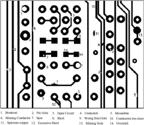
Defect Types and Their Impact
| Defect Type | Impact |
|---|---|
| Short Circuits | Unintended connections between conductors, leading to malfunction or failure |
| Open Circuits | Broken or disconnected conductors, resulting in loss of signal or power |
| Incorrect Trace Width | Altered electrical characteristics, such as resistance and current-carrying capacity |
| Delamination | Separation of PCB layers, causing mechanical and electrical issues |
| Component Misalignment | Poor connections, short circuits, and mechanical stress on the PCB |
Frequently Asked Questions (FAQ)
1. What are the most common causes of PCB defects?
The most common causes of PCB defects include incorrect design, contamination, improper etching, inadequate soldering, and component misalignment.
2. How can I ensure the quality of my PCB design?
To ensure the quality of your PCB design, follow the manufacturer’s guidelines and industry standards, use appropriate design tools and software, and perform thorough design reviews and simulations.
3. What are the consequences of using low-quality materials in PCB manufacturing?
Using low-quality materials can result in defects such as delamination, warping, and poor electrical performance, leading to reduced reliability and potential failure of the end product.
4. How can I minimize human errors in the PCB manufacturing process?
To minimize human errors, provide comprehensive training to operators and technicians, implement standardized work instructions and checklists, and use error-proofing techniques like poka-yoke.
5. What are the benefits of implementing automated testing and inspection in PCB manufacturing?
Implementing automated testing and inspection, such as AOI and X-ray inspection, helps detect defects more effectively, ensures consistency, and reduces the reliance on manual inspection, ultimately improving the overall quality of the manufactured PCBs.
In conclusion, understanding the common reasons for PCB manufacturing defects and implementing appropriate solutions can significantly improve the quality, reliability, and performance of PCBs. By following best practices in design, material selection, manufacturing processes, and quality control, manufacturers can minimize defects and deliver high-quality PCBs that meet the ever-increasing demands of modern electronics.
No responses yet