Introduction to RF PCB Design
Designing printed circuit boards (PCBs) for radio frequency (RF) and microwave applications is a complex and challenging task. Unlike traditional PCB design, which deals with lower frequencies and digital signals, RF PCB design requires a deep understanding of high-frequency behavior, signal integrity, and electromagnetic compatibility (EMC). This article will delve into the intricacies of RF PCB design, exploring the various factors that make it so difficult and providing insights into best practices and techniques to overcome these challenges.
Key Challenges in RF PCB Design
Signal Integrity
One of the primary challenges in RF PCB design is maintaining signal integrity. At high frequencies, signals are more susceptible to distortion, attenuation, and interference. These issues can arise from various sources, such as impedance mismatches, parasitic capacitances, and inductances. To ensure signal integrity, designers must carefully consider factors such as trace widths, lengths, spacing, and routing techniques.
Impedance Matching
Impedance matching is crucial in RF PCB design to minimize reflections and ensure maximum power transfer. Mismatched impedances can lead to signal reflections, causing standing waves and reducing the overall system performance. Designers must calculate and control the characteristic impedance of transmission lines, which depends on factors such as the dielectric constant of the substrate, trace width, and height above the ground plane.
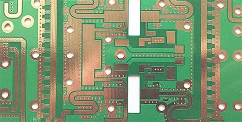
Microstrip and Stripline Transmission Lines
Two common types of transmission lines used in RF PCB design are microstrip and stripline. Microstrip lines consist of a conductive trace on the top layer of the PCB, with a ground plane on the bottom layer. Stripline, on the other hand, has the conductive trace sandwiched between two ground planes. Each type has its advantages and disadvantages in terms of impedance control, signal isolation, and manufacturing complexity.
| Transmission Line | Advantages | Disadvantages |
|---|---|---|
| Microstrip | – Easier to manufacture – Lower cost – Allows for component placement on top layer |
– Higher radiation and coupling – Less isolation between signals – Dispersion at higher frequencies |
| Stripline | – Better isolation between signals – Lower radiation and coupling – More consistent impedance |
– More complex to manufacture – Higher cost – Requires vias for component placement |
Electromagnetic Compatibility (EMC)
EMC is another critical aspect of RF PCB design. RF circuits are prone to electromagnetic interference (EMI), both as sources and victims. EMI can cause unintended radiation, crosstalk, and coupling between different parts of the circuit, leading to performance degradation and even system failure. Designers must employ various techniques to mitigate EMI, such as proper grounding, shielding, and filtering.
Grounding Techniques
Proper grounding is essential in RF PCB design to provide a low-impedance return path for high-frequency currents and to minimize ground bounce and voltage differences across the board. Designers often use ground planes, which are large copper areas on one or more layers of the PCB, to create a stable reference for signals. Additionally, techniques such as split ground planes, moats, and stitching capacitors can be used to isolate sensitive circuits and prevent ground loops.
Shielding and Filtering
Shielding is another effective method to reduce EMI in RF PCB design. Shielding involves enclosing sensitive circuits or components within a conductive barrier to block external electromagnetic fields. This can be achieved through the use of metal enclosures, conductive gaskets, or even by placing grounded vias around critical areas on the PCB.
Filtering is used to suppress unwanted high-frequency noise and harmonics in RF circuits. Common filtering techniques include the use of low-pass, high-pass, and band-pass filters, as well as decoupling capacitors and ferrite beads. These components help to attenuate noise and prevent it from propagating throughout the system.
Component Placement and Routing
Component placement and routing are critical aspects of RF PCB design that can significantly impact performance. At high frequencies, the physical layout of components and traces becomes increasingly important. Designers must consider factors such as component proximity, trace lengths, and routing angles to minimize parasitic effects and maintain signal integrity.
Component Proximity
In RF PCB design, the placement of components relative to each other can have a significant impact on performance. Components that operate at high frequencies should be placed as close together as possible to minimize trace lengths and reduce parasitic inductances. However, designers must also consider the potential for crosstalk and coupling between adjacent components, which can be mitigated through proper spacing and shielding.
Trace Routing
Trace routing in RF PCB design requires careful consideration of factors such as trace width, length, and geometry. At high frequencies, the wavelength of signals becomes comparable to the dimensions of the PCB, leading to transmission line effects. Designers must ensure that traces are properly sized and routed to maintain the desired characteristic impedance and minimize reflections.
One important aspect of trace routing is the use of smooth, gradual bends instead of sharp corners. Sharp corners can cause reflections and impedance discontinuities, leading to signal degradation. Designers should use curved or mitered bends to maintain a consistent impedance along the trace.
Material Selection
The choice of materials used in RF PCB design can have a significant impact on performance. The dielectric constant (Dk) and dissipation factor (Df) of the substrate material affect the propagation velocity, impedance, and loss of high-frequency signals. Low-loss materials, such as PTFE (Teflon) and Rogers laminates, are often used in RF PCB design to minimize dielectric losses and maintain signal integrity.
| Material | Dielectric Constant (Dk) | Dissipation Factor (Df) | Advantages | Disadvantages |
|---|---|---|---|---|
| FR-4 | 4.3-4.7 | 0.02 | – Low cost – Widely available |
– Higher losses at high frequencies – Moisture absorption |
| Rogers RO4350B | 3.48 | 0.0037 | – Low loss – Stable Dk – Low moisture absorption |
– Higher cost – More complex processing |
| PTFE (Teflon) | 2.1 | 0.0002 | – Lowest loss – Stable Dk – Low moisture absorption |
– Highest cost – Difficult to process |
In addition to the substrate material, designers must also consider the properties of the conductor material, such as copper thickness and surface roughness. Thicker copper traces can help to reduce losses, while smoother surfaces can minimize skin effect and improve signal propagation.

Best Practices in RF PCB Design
To overcome the challenges associated with RF PCB design, designers can employ various best practices and techniques. These include:
- Use a solid ground plane to provide a low-impedance return path and minimize ground bounce.
- Keep trace lengths as short as possible to reduce parasitic inductances and capacitances.
- Use appropriate transmission line structures, such as microstrip or stripline, depending on the requirements for impedance control and signal isolation.
- Maintain consistent trace widths and spacing to ensure a uniform characteristic impedance.
- Use smooth, gradual bends instead of sharp corners to minimize reflections and impedance discontinuities.
- Place decoupling capacitors close to active components to reduce power supply noise and improve signal integrity.
- Use shielding and filtering techniques to mitigate EMI and prevent interference between different parts of the circuit.
- Select low-loss substrate materials and consider the impact of dielectric constant and dissipation factor on high-frequency performance.
- Perform comprehensive simulations and analysis to validate the design and identify potential issues before fabrication.
- Collaborate closely with the PCB fabricator to ensure that the design can be manufactured reliably and cost-effectively.

Frequently Asked Questions (FAQ)
-
Q: What is the main difference between RF PCB design and traditional PCB design?
A: The main difference between RF PCB design and traditional PCB design is the frequency range of the signals involved. RF PCB design deals with high-frequency signals, typically in the range of hundreds of megahertz to several gigahertz, which require special considerations for signal integrity, impedance matching, and electromagnetic compatibility. -
Q: Why is impedance matching important in RF PCB design?
A: Impedance matching is important in RF PCB design to ensure maximum power transfer and minimize signal reflections. When impedances are mismatched, a portion of the signal energy is reflected back to the source, causing standing waves and reducing the overall system performance. By matching the impedances of the source, transmission line, and load, designers can optimize signal propagation and minimize losses. -
Q: What are some common techniques for mitigating EMI in RF PCB design?
A: Some common techniques for mitigating EMI in RF PCB design include proper grounding, shielding, and filtering. Grounding techniques, such as the use of ground planes and stitching capacitors, help to provide a low-impedance return path for high-frequency currents and minimize ground bounce. Shielding involves enclosing sensitive circuits within a conductive barrier to block external electromagnetic fields, while filtering helps to suppress unwanted high-frequency noise and harmonics. -
Q: How does the choice of substrate material affect RF PCB performance?
A: The choice of substrate material can have a significant impact on RF PCB performance. The dielectric constant (Dk) and dissipation factor (Df) of the substrate material affect the propagation velocity, impedance, and loss of high-frequency signals. Low-loss materials, such as PTFE (Teflon) and Rogers laminates, are often used in RF PCB design to minimize dielectric losses and maintain signal integrity. -
Q: What are some best practices for component placement and routing in RF PCB design?
A: Some best practices for component placement and routing in RF PCB design include keeping trace lengths as short as possible, maintaining consistent trace widths and spacing, using smooth bends instead of sharp corners, and placing decoupling capacitors close to active components. Designers should also consider the proximity of components to minimize crosstalk and coupling, and use appropriate transmission line structures to ensure proper impedance control and signal isolation.

Conclusion
Designing RF and Microwave PCBs is a complex and challenging task that requires a deep understanding of high-frequency behavior, signal integrity, and electromagnetic compatibility. Designers must contend with various factors, such as impedance matching, EMI, component placement, and material selection, to ensure optimal performance and reliability.
By employing best practices and techniques, such as proper grounding, shielding, filtering, and trace routing, designers can overcome the difficulties associated with RF PCB design. Additionally, the use of advanced simulation tools and close collaboration with PCB fabricators can help to validate designs and ensure successful manufacturing.
As the demand for high-speed wireless communication systems continues to grow, the importance of effective RF PCB design will only increase. By staying up-to-date with the latest techniques and technologies, designers can create robust and reliable RF circuits that meet the ever-evolving needs of the industry.
No responses yet