Introduction to PCBs
A Printed Circuit Board (PCB) is a fundamental component in modern electronics. It is a flat board made of insulating material, such as fiberglass or composite epoxy, with conductive pathways etched or printed onto its surface. These pathways, also known as traces, connect various electronic components, such as resistors, capacitors, and integrated circuits, to form a complete electrical circuit.
PCBs have revolutionized the electronics industry by providing a reliable, compact, and cost-effective means of connecting electronic components. They are used in almost every electronic device, from smartphones and computers to medical equipment and aerospace systems.
Types of PCBs
There are several types of PCBs, each with its own unique characteristics and applications:
-
Single-Sided PCBs: These have conductive traces on only one side of the board. They are the simplest and most cost-effective type of PCB, suitable for low-complexity circuits.
-
Double-sided PCBs: These have conductive traces on both sides of the board, allowing for more complex circuits and higher component density. The two sides are connected through holes called vias.
-
Multi-layer PCBs: These consist of multiple layers of conductive traces separated by insulating layers. They offer the highest component density and are used in complex, high-performance applications.
-
Flexible PCBs: These are made of flexible materials, such as polyimide, allowing them to bend and conform to various shapes. They are often used in wearable electronics and applications where space is limited.
-
Rigid-Flex PCBs: These combine rigid and flexible sections, providing the benefits of both types of PCBs. They are used in applications that require both high component density and flexibility.
What is a Blank PCB?
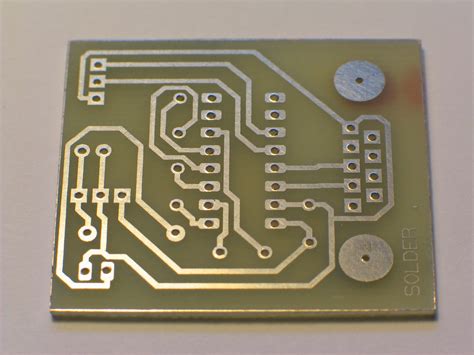
A blank PCB, also known as a bare or unpopulated PCB, is a printed circuit board without any electronic components soldered onto it. It consists of the insulating substrate, conductive traces, and any necessary features such as holes, pads, and silkscreen markings.
Blank PCBs are the starting point for creating custom electronic circuits. They can be purchased from PCB manufacturers or made at home using various methods, such as etching or milling.
Advantages of Using Blank PCBs
Using blank PCBs offers several advantages over other prototyping methods:
-
Customization: Blank PCBs allow you to create custom circuits tailored to your specific needs, providing flexibility in design and functionality.
-
Reliability: PCBs offer a more reliable and durable connection between components compared to breadboards or wire-wrap techniques.
-
Compact size: PCBs enable the creation of compact, space-saving circuits, which is essential for many modern electronic devices.
-
Repeatability: Once a PCB design is finalized, it can be easily replicated, ensuring consistency across multiple units.

How to Make a Blank PCB
Making a blank PCB involves several steps, from designing the circuit to fabricating the board. Here’s an overview of the process:
Step 1: Circuit Design
The first step in making a blank PCB is to design the circuit. This involves creating a schematic diagram that shows the connections between the various components. You can use electronic design automation (EDA) software, such as KiCad, Eagle, or Altium Designer, to create the schematic.
Once the schematic is complete, you need to create a PCB layout that translates the schematic into a physical board design. The layout software will help you arrange the components and route the traces while adhering to design rules and constraints.
Step 2: PCB Fabrication
After finalizing the PCB layout, you can proceed with the fabrication process. There are two main methods for making blank PCBs:
-
Etching: This method involves transferring the PCB layout onto a copper-clad board using a photoresist process and then etching away the unwanted copper using a chemical solution, such as ferric chloride. This leaves behind the desired conductive traces.
-
Milling: This method uses a CNC (computer numeric control) machine to mechanically remove the unwanted copper from the board, leaving behind the desired traces. Milling is suitable for prototyping and low-volume production.
Step 3: PCB Finishing
After fabricating the blank PCB, you may need to perform some additional steps to prepare it for component assembly:
-
Drilling: If your PCB requires through-hole components, you’ll need to drill holes at the appropriate locations using a drill press or a CNC machine.
-
Surface Finish: To protect the copper traces from oxidation and improve solderability, you can apply a surface finish, such as HASL (Hot Air Solder Leveling), lead-free HASL, or ENIG (Electroless Nickel Immersion Gold).
-
Silkscreen: You can add silkscreen markings to the PCB to indicate component placement, polarity, and other important information. This is typically done using a silkscreen printing process.

Designing Your Own PCB
Designing your own PCB can be a rewarding experience, allowing you to create custom circuits for your projects. Here are some tips to help you get started:
-
Start with a schematic: Always begin by creating a schematic diagram of your circuit. This will help you understand the connections between components and serve as a blueprint for your PCB layout.
-
Choose the right software: Select an EDA software package that suits your needs and skill level. Some popular options include KiCad (free and open-source), Eagle (free for small projects), and Altium Designer (paid, professional-grade).
-
Learn PCB design rules: Familiarize yourself with the basic PCB design rules, such as minimum trace width, clearance, and hole size. These rules ensure that your PCB can be manufactured reliably and function correctly.
-
Use a modular approach: Break down complex circuits into smaller, modular sections. This makes the design process more manageable and allows for easier debugging and modification.
-
Test and iterate: Before sending your design for fabrication, double-check your schematic and layout for errors. If possible, prototype your circuit on a breadboard to verify its functionality. Make necessary changes and iterate until you’re satisfied with the design.

Conclusion
Blank PCBs are an essential component in the world of electronics, providing a foundation for creating custom circuits. Understanding the different types of PCBs and the process of making them can help you bring your electronic projects to life.
Whether you choose to design your own PCB or work with a professional PCB manufacturer, the key to success is careful planning, attention to detail, and a willingness to learn and iterate. With the right tools and knowledge, you can create PCBs that are reliable, efficient, and tailored to your specific needs.
Frequently Asked Questions (FAQ)
-
Q: What is the difference between a blank PCB and a populated PCB?
A: A blank PCB is a printed circuit board without any electronic components soldered onto it, while a populated PCB has components attached to it, ready for use in an electronic device. -
Q: Can I make a PCB at home without using chemicals?
A: Yes, you can make a PCB at home using the milling method, which involves using a CNC machine to mechanically remove unwanted copper from the board. This method does not require the use of chemicals like etching does. -
Q: What software can I use to design a PCB?
A: There are several electronic design automation (EDA) software packages available for PCB design, including KiCad (free and open-source), Eagle (free for small projects), and Altium Designer (paid, professional-grade). -
Q: What are the basic PCB design rules I should be aware of?
A: Some basic PCB design rules include minimum trace width, clearance between traces, minimum hole size, and component placement guidelines. These rules ensure that your PCB can be manufactured reliably and function correctly. -
Q: Can I use a blank PCB for both through-hole and surface-mount components?
A: Yes, a blank PCB can be designed to accommodate both through-hole and surface-mount components. The key is to design the board with the appropriate pad sizes, hole sizes (for through-hole components), and component placement in mind.
No responses yet