What is PCB Fabrication?
PCB fabrication refers to the process of creating printed circuit boards that electrically connect electronic components using conductive pathways, tracks or signal traces etched from laminated sheets of copper. The process involves several steps, including design, printing, etching, drilling, plating, and finishing.
PCB Fabrication Process
The PCB fabrication process typically includes the following steps:
-
PCB Design: The first step is to design the PCB layout using computer-aided design (CAD) software such as Altium, Eagle, or KiCad. The design includes the placement of components, routing of traces, and creation of soldermask and silkscreen layers.
-
Printing: Once the design is complete, the PCB layout is printed onto a transparent film or directly onto the copper-clad laminate using a plotter or laser printer.
-
Etching: The printed PCB undergoes an etching process where the unwanted copper is removed, leaving only the desired conductive traces. This is typically done using a chemical etching process.
-
Drilling: Holes are drilled into the PCB to allow for the mounting of components and the creation of vias (electrical connections between layers).
-
Plating: The drilled holes are plated with a conductive material, usually copper, to create electrical connections between the layers.
-
Soldermask Application: A soldermask layer is applied to the PCB to protect the copper traces and prevent solder bridging.
-
Silkscreen Printing: A silkscreen layer is printed onto the PCB to add text, logos, and component identifiers.
-
Surface Finish: A surface finish, such as HASL (Hot Air Solder Leveling), ENIG (Electroless Nickel Immersion Gold), or OSP (Organic Solderability Preservative), is applied to protect the exposed copper and enhance solderability.
-
Electrical Testing: The fabricated PCBs undergo electrical testing to ensure they function as intended and meet the required specifications.
-
Cutting and Packaging: The PCB panel is cut into individual boards, and the finished PCBs are packaged for shipping.

Types of PCBs
There are several types of PCBs, each with its own characteristics and manufacturing process:
Single-Layer PCBs
Single-layer PCBs have conductive traces on only one side of the board. They are the simplest and most cost-effective type of PCB.
Double-Layer PCBs
Double-layer PCBs have conductive traces on both sides of the board, allowing for more complex circuits and higher component density. The two layers are connected using vias.
Multi-Layer PCBs
Multi-layer PCBs have three or more conductive layers, separated by insulating layers. They offer the highest component density and are used in complex electronic devices.
Flexible PCBs
Flexible PCBs are made from flexible materials, such as polyimide, and can bend and fold to fit into tight spaces or conform to curved surfaces.
Rigid-Flex PCBs
Rigid-flex PCBs combine rigid and flexible sections, allowing for both stability and flexibility in the same board.

PCB Materials
The choice of PCB material depends on the specific application, required performance, and cost considerations. Common PCB materials include:
-
FR-4: A glass-reinforced epoxy laminate, FR-4 is the most widely used PCB material due to its good mechanical and electrical properties, and low cost.
-
High-Frequency Materials: For high-frequency applications, such as RF and microwave circuits, special materials like Rogers, Teflon, and ceramic-based laminates are used to minimize signal loss and maintain signal integrity.
-
Metal Core: Metal core PCBs have a metal base, usually aluminum, to enhance heat dissipation in high-power applications.
-
Polyimide: Polyimide is used for flexible PCBs due to its high heat resistance, flexibility, and durability.

PCB Design Considerations
When designing a PCB, several factors must be considered to ensure optimal performance, manufacturability, and cost-effectiveness:
Component Placement
Proper component placement is crucial for signal integrity, thermal management, and manufacturing efficiency. Consider factors such as signal flow, power distribution, and mechanical constraints when placing components.
Trace Routing
Trace routing involves creating the conductive paths that connect components on the PCB. Ensure proper trace width, spacing, and impedance control to minimize signal integrity issues and electromagnetic interference (EMI).
Vias and Through-Holes
Vias and through-holes are used to create electrical connections between layers in multi-layer PCBs. Minimize the number of vias and optimize their placement to reduce signal degradation and manufacturing costs.
Thermal Management
Effective thermal management is essential to prevent overheating and ensure reliable operation. Use thermal relief pads, copper pours, and heat sinks to dissipate heat from high-power components.
Design for Manufacturing (DFM)
Design your PCB with manufacturing in mind to minimize potential issues and reduce costs. Follow the manufacturer’s design guidelines, use standard component sizes and footprints, and provide adequate spacing and clearances.
PCB Manufacturing Standards
Adhering to industry standards ensures consistency, reliability, and compatibility in PCB manufacturing. Some key standards include:
- IPC-A-600: Acceptability of Printed Boards
- IPC-2221: Generic Standard on Printed Board Design
- IPC-6012: Qualification and Performance Specification for Rigid Printed Boards
- IPC-6013: Qualification and Performance Specification for Flexible Printed Boards
- IPC-7351: Generic Requirements for Surface Mount Design and Land Pattern Standard
Choosing a PCB Manufacturer
Selecting the right PCB manufacturer is crucial for ensuring the quality, reliability, and timely delivery of your PCBs. Consider the following factors when choosing a PCB manufacturer:
- Capabilities: Ensure the manufacturer has the necessary equipment, processes, and expertise to fabricate your specific type of PCB.
- Quality Control: Look for manufacturers with strict quality control processes and certifications such as ISO 9001, UL, and IPC.
- Lead Time: Consider the manufacturer’s lead time and ability to meet your production schedule.
- Cost: Obtain quotes from multiple manufacturers and compare costs, but don’t sacrifice quality for lower prices.
- Customer Support: Choose a manufacturer with responsive customer support and clear communication channels.
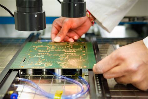
PCB Testing and Inspection
Thorough testing and inspection are essential to ensure the quality and reliability of fabricated PCBs. Common testing and inspection methods include:
- Visual Inspection: Manual or automated visual inspection to identify surface defects, misalignments, and contamination.
- Automated Optical Inspection (AOI): Uses cameras and image processing software to detect surface defects and component placement issues.
- X-Ray Inspection: Non-destructive testing method to inspect hidden solder joints and internal structures.
- Electrical Testing: Includes continuity testing, insulation resistance testing, and functional testing to verify electrical performance.
- Microsectioning: Destructive testing method that involves cross-sectioning the PCB to examine internal structures and plating quality.
Common PCB Defects and Troubleshooting
Despite stringent quality control measures, PCB defects can still occur during fabrication. Some common PCB defects include:
- Short Circuits: Unintended electrical connections between traces or components.
- Open Circuits: Broken or missing connections between traces or components.
- Solder Bridges: Excess solder that creates a short circuit between adjacent pads or traces.
- Copper Delamination: Separation of the copper layer from the substrate material.
- Drill Misalignment: Misaligned or improperly sized holes that affect component placement and soldering.
Troubleshooting PCB defects involves a systematic approach to identify and correct the root cause of the issue. This may include visual inspection, electrical testing, and microscopic analysis.
PCB Fabrication Cost Factors
The cost of PCB fabrication depends on several factors, including:
- Board Size: Larger boards require more material and processing time, increasing the cost.
- Layer Count: Multi-layer boards are more complex and expensive to manufacture than single or double-layer boards.
- Material: The choice of PCB material affects the cost, with specialized materials like high-frequency laminates being more expensive than standard FR-4.
- Quantity: Higher production volumes often result in lower per-unit costs due to economies of scale.
- Surface Finish: The choice of surface finish, such as HASL, ENIG, or OSP, impacts the overall cost.
- Turnaround Time: Faster turnaround times may incur additional costs due to expedited processing and shipping.
Future Trends in PCB Fabrication
As electronic devices continue to advance, PCB fabrication technologies must evolve to keep pace. Some emerging trends in PCB fabrication include:
- Miniaturization: The demand for smaller, more compact electronic devices is driving the development of advanced PCB fabrication techniques, such as high-density interconnect (HDI) and embedded components.
- 3D Printing: Additive manufacturing technologies are being explored for PCB fabrication, enabling the creation of complex, three-dimensional structures and reducing waste.
- Eco-Friendly Materials: There is a growing emphasis on using environmentally friendly PCB materials and processes to reduce the industry’s ecological footprint.
- Flexible and Stretchable Electronics: The development of flexible and stretchable PCBs is enabling new applications in wearable devices, medical implants, and soft robotics.
Frequently Asked Questions (FAQ)
-
What is the difference between PCB assembly and PCB fabrication?
PCB fabrication refers to the process of manufacturing the bare printed circuit board, while PCB assembly involves soldering components onto the fabricated board to create a functional electronic assembly. -
How long does PCB fabrication typically take?
The lead time for PCB fabrication depends on factors such as the complexity of the design, the chosen manufacturer, and the order quantity. Standard lead times can range from a few days to several weeks. -
What is the minimum feature size in PCB fabrication?
The minimum feature size depends on the manufacturer’s capabilities and the chosen fabrication technology. Advanced PCB fabrication techniques can achieve feature sizes as small as 50 microns (0.05 mm) or less. -
Can I fabricate PCBs at home?
While it is possible to fabricate simple PCBs at home using methods like etching or milling, the process can be challenging and may not yield professional-quality results. For complex designs and high-reliability applications, it is recommended to use a professional PCB fabrication service. -
What is the typical lifespan of a PCB?
The lifespan of a PCB depends on factors such as the materials used, the operating environment, and the level of stress the board is subjected to. With proper design, fabrication, and use, a PCB can last for many years or even decades.
Conclusion
PCB fabrication is a complex process that involves multiple steps, materials, and technologies. Understanding the fundamentals of PCB fabrication is essential for anyone involved in electronics design and manufacturing. By following best practices in PCB design, selecting the right manufacturer, and implementing thorough testing and inspection, you can ensure the quality, reliability, and cost-effectiveness of your printed circuit boards.
As electronic devices continue to evolve, PCB fabrication technologies must adapt to meet new challenges and opportunities. Staying informed about the latest trends and advancements in PCB fabrication will help you stay competitive in this dynamic industry.
Table: Common PCB Materials and Their Properties
| Material | Dielectric Constant | Dissipation Factor | Tg (°C) | Thermal Conductivity (W/mK) | Applications |
|---|---|---|---|---|---|
| FR-4 | 4.2-4.5 | 0.02 | 130-140 | 0.3 | General-purpose, low-cost PCBs |
| Rogers 4350 | 3.48 | 0.0037 | >280 | 0.62 | High-frequency, low-loss PCBs |
| Polyimide | 3.4-3.5 | 0.002-0.003 | >250 | 0.1-0.2 | Flexible PCBs, high-temperature applications |
| Alumina | 9.8-10.0 | 0.0001-0.0004 | N/A | 24-30 | High-frequency, high-power PCBs |
| PTFE | 2.1 | 0.0002 | 327 | 0.25 | High-frequency, low-loss PCBs |
Table: PCB Surface Finishes Comparison
| Surface Finish | Shelf Life | Solderability | Flatness | Cost | RoHS Compliance |
|---|---|---|---|---|---|
| HASL | 12 months | Good | Fair | Low | Yes |
| ENIG | 12 months | Excellent | Good | High | Yes |
| OSP | 6 months | Good | Excellent | Low | Yes |
| Immersion Tin | 12 months | Good | Good | Low | Yes |
| Immersion Silver | 12 months | Excellent | Excellent | High | Yes |
No responses yet