Understanding PCB Copper Thickness and Its Importance
Printed Circuit Boards (PCBs) are the backbone of modern electronics, providing a platform for connecting and integrating various components. One of the critical aspects of PCB Design and manufacturing is the copper thickness, which plays a significant role in determining the board’s electrical and thermal properties. In this article, we will delve into the topic of tolerances on copper thickness on a PCB, exploring its importance, measurement methods, factors affecting it, and best practices for maintaining accurate copper thickness.
What is PCB Copper Thickness?
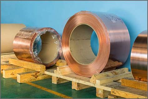
PCB copper thickness refers to the thickness of the copper layer deposited on the insulating substrate of a printed circuit board. The copper layer is responsible for conducting electrical signals between components and providing a heat dissipation path. Copper thickness is typically measured in ounces per square foot (oz/ft²) or micrometers (µm).
Common PCB copper thicknesses include:
| Copper Weight (oz/ft²) | Thickness (µm) |
|---|---|
| 0.5 oz | 17.5 µm |
| 1 oz | 35 µm |
| 2 oz | 70 µm |
| 3 oz | 105 µm |
Importance of Accurate Copper Thickness
Maintaining accurate copper thickness is crucial for several reasons:
-
Electrical Performance: The thickness of the copper layer directly influences the electrical resistance and current-carrying capacity of the PCB traces. Insufficient copper thickness can lead to higher resistance, causing signal integrity issues and power loss.
-
Thermal Management: Thicker copper layers provide better heat dissipation, helping to prevent thermal stress on components and improve the overall reliability of the PCB.
-
Manufacturing Consistency: Ensuring consistent copper thickness across the board is essential for maintaining uniform electrical and thermal properties, reducing the risk of defects and failures.
Measuring PCB Copper Thickness
Methods for Measuring Copper Thickness
There are several methods for measuring PCB copper thickness, each with its own advantages and limitations:
-
X-ray Fluorescence (XRF): XRF is a non-destructive method that uses X-rays to measure the thickness of the copper layer. It provides accurate results and can measure multiple points on the board quickly.
-
Cross-Sectional Analysis: This destructive method involves cutting a small section of the PCB and examining it under a microscope. While it provides a direct measurement of the copper thickness, it is time-consuming and requires destroying a portion of the board.
-
Electrical Resistance Measurement: This method involves measuring the electrical resistance of a trace and calculating the copper thickness based on the trace’s dimensions and the material’s resistivity. It is a non-destructive method but may not be as accurate as XRF or cross-sectional analysis.
Factors Affecting Copper Thickness Measurement
Several factors can influence the accuracy of copper thickness measurements:
-
Surface Roughness: The surface roughness of the copper layer can affect the measurement results, particularly when using XRF. Rough surfaces may lead to over-estimation of the copper thickness.
-
Plating Variations: Uneven plating or variations in the plating process can result in non-uniform copper thickness across the board, making accurate measurements more challenging.
-
Measurement Location: The location of the measurement points on the PCB can impact the results, as copper thickness may vary slightly across the board due to manufacturing tolerances.

Tolerances on PCB Copper Thickness
Industry Standards for Copper Thickness Tolerances
The electronics industry has established standards for copper thickness tolerances to ensure consistency and reliability in PCB manufacturing. The most common standards include:
-
IPC-6012: This standard specifies the acceptable range of copper thickness for different copper weights. For example, a 1 oz copper has a nominal thickness of 35 µm, with a tolerance of ±20%.
-
IPC-600: This standard provides guidelines for the visual inspection of PCBs, including the assessment of copper thickness uniformity.
| Copper Weight (oz/ft²) | Nominal Thickness (µm) | Tolerance (IPC-6012) |
|---|---|---|
| 0.5 oz | 17.5 µm | ±20% |
| 1 oz | 35 µm | ±20% |
| 2 oz | 70 µm | ±20% |
| 3 oz | 105 µm | ±20% |
Factors Affecting Copper Thickness Tolerances
Several factors can impact the copper thickness tolerances on a PCB:
-
Manufacturing Process: The choice of manufacturing process, such as electroplating or foil lamination, can influence the uniformity and consistency of the copper thickness.
-
Board Design: The complexity of the board design, including the presence of fine-pitch traces and high-density components, can make it more challenging to maintain tight copper thickness tolerances.
-
Material Selection: The quality and consistency of the raw materials used in PCB manufacturing, such as the copper foil and the insulating substrate, can affect the final copper thickness and its tolerances.

Best Practices for Maintaining Accurate Copper Thickness
To ensure accurate and consistent copper thickness on PCBs, consider the following best practices:
-
Design for Manufacturability: When designing the PCB, consider the limitations of the manufacturing process and the achievable copper thickness tolerances. Avoid overly aggressive designs that may push the limits of the manufacturing capabilities.
-
Supplier Selection: Choose reputable PCB Manufacturers with a proven track record of producing boards with consistent copper thickness. Verify their Quality Control processes and adherence to industry standards.
-
Regular Monitoring: Implement a regular monitoring program to measure and track copper thickness across multiple production runs. This helps identify any deviations or trends that may indicate issues with the manufacturing process.
-
Process Optimization: Work closely with the PCB manufacturer to optimize the manufacturing process for consistent copper thickness. This may involve fine-tuning the plating parameters, improving the copper etching process, or implementing better process controls.

Frequently Asked Questions (FAQ)
-
What is the most common copper thickness used in PCBs?
The most common copper thickness used in PCBs is 1 oz/ft², which corresponds to a nominal thickness of 35 µm. This thickness provides a good balance between electrical performance, thermal management, and manufacturability. -
Can I use different copper thicknesses on the same PCB?
Yes, it is possible to use different copper thicknesses on the same PCB. This is often done to optimize the electrical and thermal properties of specific traces or areas of the board. However, it may increase the manufacturing complexity and cost. -
What happens if the copper thickness is too low?
If the copper thickness is too low, it can lead to several issues, such as increased electrical resistance, reduced current-carrying capacity, and poor thermal dissipation. This can result in signal integrity problems, power loss, and potential reliability issues. -
How can I ensure consistent copper thickness across multiple PCB production runs?
To ensure consistent copper thickness across multiple production runs, implement a regular monitoring program to measure and track copper thickness. Work closely with the PCB manufacturer to optimize the manufacturing process and maintain tight process controls. Additionally, choose reputable suppliers with a proven track record of producing boards with consistent copper thickness. -
Are there any alternative materials to copper for PCB traces?
While copper is the most common material used for PCB traces, there are some alternatives, such as silver, gold, and aluminum. However, these materials are generally more expensive and may have different electrical and thermal properties compared to copper. Copper remains the preferred choice for most PCB Applications due to its excellent conductivity, thermal performance, and cost-effectiveness.
Conclusion
Tolerances on copper thickness on a PCB play a crucial role in ensuring the electrical performance, thermal management, and overall reliability of the board. Understanding the importance of accurate copper thickness, the methods for measuring it, and the factors affecting it is essential for designers, manufacturers, and quality control professionals.
By adhering to industry standards, implementing best practices for maintaining accurate copper thickness, and working closely with reputable PCB manufacturers, it is possible to achieve consistent and reliable results in PCB production. As the demands for high-performance electronics continue to grow, the importance of tight tolerances on copper thickness will only increase, driving further advancements in PCB design and manufacturing technologies.
No responses yet