Introduction to PCB fabrication
Printed Circuit Boards (PCBs) are the backbone of modern electronics. They provide a platform for electrical components to be mounted and connected, enabling the creation of complex circuits that power our devices. The PCB fabrication process involves several steps, each of which is critical to ensuring the quality and reliability of the final product. In this article, we will explore the various steps involved in PCB fabrication and the techniques used in PCB manufacturing.
PCB Design and Layout
The first step in the PCB fabrication process is the design and layout of the circuit board. This involves creating a schematic diagram of the circuit, which shows the electrical connections between components. The schematic is then used to create a physical layout of the board, which determines the placement of components and the routing of the copper traces that connect them.
PCB Design Software
PCB design software is used to create the schematic and layout of the board. There are several popular PCB design software packages available, including:
| Software | Description |
|---|---|
| Altium Designer | A comprehensive PCB design package with advanced features for high-speed design and simulation. |
| Eagle | A popular PCB design software for hobbyists and small businesses, with a free version available. |
| KiCad | An Open-Source PCB design software with a growing community of users and developers. |
PCB Layout Considerations
When designing the layout of a PCB, there are several factors to consider, including:
- Component placement: Components should be placed in a way that minimizes the length of copper traces and reduces the risk of electromagnetic interference (EMI).
- Trace width and spacing: The width and spacing of copper traces should be carefully designed to ensure proper signal integrity and to avoid short circuits.
- Ground planes: Ground planes are used to provide a low-impedance return path for signals and to reduce EMI.
- Thermal management: The layout should be designed to ensure proper heat dissipation, especially for high-power components.
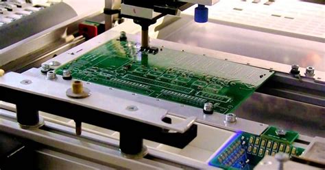
PCB Fabrication Process
Once the PCB design is complete, the fabrication process can begin. The fabrication process involves several steps, each of which is critical to ensuring the quality and reliability of the final product.
Step 1: Material Selection
The first step in the PCB fabrication process is to select the appropriate material for the board. The most common material used for PCBs is FR-4, which is a glass-reinforced epoxy laminate. Other materials, such as polyimide or PTFE, may be used for high-frequency or high-temperature applications.
Step 2: Copper Clad Laminate
The selected material is then coated with a thin layer of copper on one or both sides, depending on the design of the board. This copper-clad laminate serves as the base for the circuit board.
Step 3: Drilling
Holes are drilled into the board to accommodate through-hole components and vias, which are used to connect different layers of the board. The drilling process is typically done using a CNC machine, which can drill holes with high precision and accuracy.
Step 4: Patterning
The copper layer is then patterned to create the desired circuit layout. This is typically done using a photolithographic process, which involves the following steps:
- The copper-clad laminate is coated with a light-sensitive photoresist material.
- The photoresist is exposed to light through a photomask, which contains the desired circuit pattern.
- The exposed photoresist is developed, leaving behind a pattern of the circuit on the copper layer.
- The unwanted copper is etched away using a chemical solution, leaving behind the desired circuit pattern.
Step 5: Plating
After patterning, the board may undergo additional plating processes to improve the conductivity and durability of the copper traces. This may include:
- Electroless plating: A thin layer of copper is deposited onto the board using a chemical process.
- Electrolytic plating: A thicker layer of copper is deposited onto the board using an electrical current.
- Solder mask application: A layer of solder mask is applied to the board to protect the copper traces and prevent short circuits.
- Silkscreen printing: Text and symbols are printed onto the board using a silkscreen process.
Step 6: Surface Finish
The final step in the PCB fabrication process is to apply a surface finish to the board. The surface finish provides protection against oxidation and improves the solderability of the board. Common surface finishes include:
| Surface Finish | Description |
|---|---|
| HASL (Hot Air Solder Leveling) | A thin layer of solder is applied to the board using hot air. |
| ENIG (Electroless Nickel Immersion Gold) | A layer of nickel is deposited onto the board, followed by a thin layer of gold. |
| OSP (Organic Solderability Preservative) | A thin layer of organic compound is applied to the board to prevent oxidation. |

PCB Manufacturing Techniques
There are several techniques used in PCB manufacturing, each with its own advantages and disadvantages.
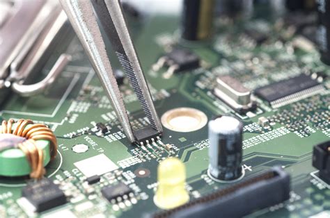
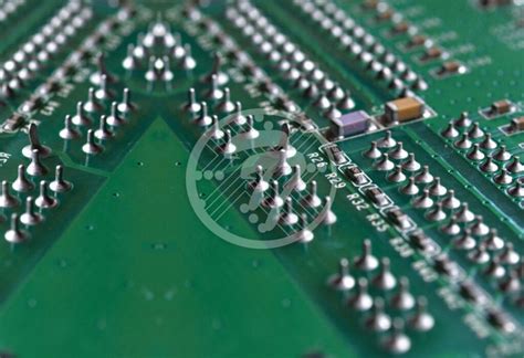
Through-Hole Technology
Through-hole technology involves drilling holes into the board and inserting components through the holes. The components are then soldered onto the board on the opposite side. Through-hole technology is reliable and sturdy, but it is also more expensive and time-consuming than other techniques.
Surface-Mount Technology (SMT)
Surface-mount technology involves mounting components directly onto the surface of the board, without the need for holes. SMT is faster and more cost-effective than through-hole technology, but it requires more precise placement of components.
Mixed Technology
Mixed technology involves using both through-hole and surface-mount components on the same board. This allows for greater flexibility in design and can be useful for boards with a mix of analog and digital components.
Quality Control in PCB Fabrication
Quality control is critical in PCB fabrication to ensure that the final product meets the required specifications and is free from defects. There are several techniques used for quality control in PCB fabrication, including:
Visual Inspection
Visual inspection involves manually inspecting the board for defects such as short circuits, open circuits, and incorrect component placement. This is typically done using a magnifying glass or microscope.
Automated Optical Inspection (AOI)
AOI involves using a camera and image processing software to automatically inspect the board for defects. AOI can detect defects that are difficult to see with the naked eye, such as hairline cracks or tiny solder bridges.
X-Ray Inspection
X-ray inspection involves using an X-ray machine to inspect the board for defects that are not visible on the surface, such as voids in solder joints or broken connections.
Electrical Testing
Electrical testing involves using specialized equipment to test the electrical properties of the board, such as resistance, capacitance, and inductance. This can help to identify defects such as short circuits or open circuits.
Frequently Asked Questions (FAQ)
What is the difference between a PCB and a printed wiring board (PWB)?
A PCB and a PWB are essentially the same thing. The term “printed wiring board” was used in the past, but “printed circuit board” is the more common term used today.
What is the typical turnaround time for PCB fabrication?
The turnaround time for PCB fabrication can vary depending on the complexity of the board and the manufacturer’s workload. Typical turnaround times range from a few days to several weeks.
Can PCBs be recycled?
Yes, PCBs can be recycled. The recycling process involves separating the different materials used in the board, such as copper, gold, and plastic, and then processing them for reuse.
What is the difference between a single-sided and a double-sided PCB?
A single-sided PCB has copper traces on only one side of the board, while a double-sided PCB has copper traces on both sides. Double-sided PCBs are more complex and expensive to manufacture, but they allow for more complex circuit designs.
What is the maximum number of layers that a PCB can have?
The maximum number of layers that a PCB can have depends on the manufacturer’s capabilities and the design requirements of the board. Some manufacturers can produce PCBs with over 50 layers, but most commercial PCBs have between 2 and 16 layers.
Conclusion
PCB fabrication is a complex process that involves several steps, each of which is critical to ensuring the quality and reliability of the final product. From material selection to surface finish, each step must be carefully controlled to ensure that the board meets the required specifications and is free from defects.
As technology continues to advance, the demand for high-quality PCBs will only continue to grow. By understanding the steps involved in PCB fabrication and the techniques used in PCB manufacturing, designers and engineers can create PCBs that are reliable, cost-effective, and meet the needs of modern electronics.
No responses yet