Introduction to PCB Fabrication
Printed Circuit Board (PCB) fabrication is a complex process that involves multiple steps and requires precise planning and execution. One of the most critical aspects of PCB fabrication is the creation of a detailed and accurate fabrication drawing. A PCB fabrication drawing, also known as a PCB layout or PCB artwork, is a graphical representation of the PCB design that serves as a blueprint for the manufacturing process.
In this article, we will delve into the world of PCB fabrication drawings, exploring their importance, key components, and best practices for creating them. We will also discuss the various file formats used for PCB fabrication drawings and how they are utilized in the manufacturing process.
The Importance of PCB Fabrication Drawings
A well-designed and accurate PCB fabrication drawing is essential for several reasons:
-
Manufacturing Accuracy: The fabrication drawing provides a clear and precise guide for the PCB manufacturer to follow during the production process. It ensures that the PCB is manufactured according to the designer’s specifications, minimizing the risk of errors and defects.
-
Communication: The fabrication drawing serves as a communication tool between the PCB designer and the manufacturer. It conveys all the necessary information, such as component placement, trace routing, and layer stackup, in a standardized format that can be easily understood by both parties.
-
Quality Control: The fabrication drawing is used as a reference for quality control checks throughout the manufacturing process. It allows the manufacturer to verify that the PCB meets the specified tolerances and requirements at each stage of production.
-
Documentation: The fabrication drawing acts as a permanent record of the PCB design. It can be used for future reference, troubleshooting, and modifications, ensuring that the design can be accurately reproduced if needed.
Key Components of a PCB Fabrication Drawing
A comprehensive PCB fabrication drawing typically includes the following components:
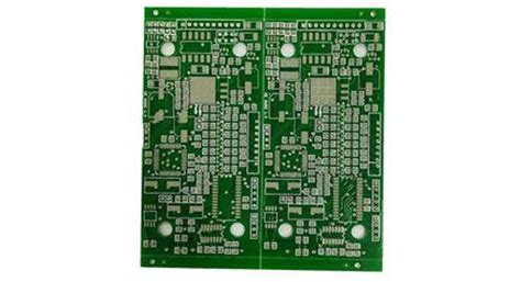
1. Board Outline
The board outline defines the physical dimensions and shape of the PCB. It includes the overall size, corner radii, and any cutouts or unique features. The board outline is usually represented by a solid line in the fabrication drawing.
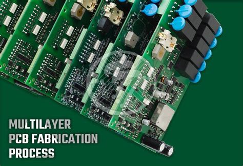
2. Layer Stackup
The layer stackup specifies the arrangement and thickness of the various layers that make up the PCB. It includes information such as the number of layers, the material used for each layer (e.g., copper, dielectric), and the thickness of each layer. The layer stackup is critical for ensuring the proper functionality and reliability of the PCB.
| Layer | Material | Thickness (mm) |
|---|---|---|
| Top Copper | Copper | 0.035 |
| Dielectric 1 | FR-4 | 0.2 |
| Inner Copper 1 | Copper | 0.035 |
| Dielectric 2 | FR-4 | 0.2 |
| Inner Copper 2 | Copper | 0.035 |
| Dielectric 3 | FR-4 | 0.2 |
| Bottom Copper | Copper | 0.035 |
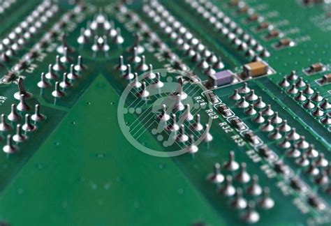
3. Drill Drawing
The drill drawing indicates the location, size, and type of all the holes in the PCB. This includes mounting holes, vias, and component holes. The drill drawing is usually provided as a separate file or layer in the fabrication drawing, using different symbols or colors to represent different hole types.
4. Copper Layers
The copper layers are the conductive layers of the PCB where the electrical connections are made. The fabrication drawing includes a separate file or layer for each copper layer, showing the trace routing, component pads, and any other copper features. The copper layers are typically represented using Gerber format, which is a standard file format for PCB fabrication.
5. Solder Mask
The solder mask is a protective coating applied to the PCB to prevent accidental short circuits and protect the copper traces from oxidation. The fabrication drawing specifies the areas where the solder mask should be applied and the color of the solder mask (e.g., green, red, blue). The solder mask layer is usually represented using Gerber format.
6. Silkscreen
The silkscreen layer contains text, logos, and other markings that are printed on the PCB for identification and assembly purposes. The fabrication drawing specifies the content and location of the silkscreen elements, as well as the color of the ink used. The silkscreen layer is also represented using Gerber format.
7. Assembly Drawing
The assembly drawing provides instructions for the placement and orientation of components on the PCB. It includes a bill of materials (BOM) that lists all the components used in the design, along with their reference designators, values, and package types. The assembly drawing may also include additional information, such as assembly notes and polarization indicators.

Best Practices for Creating PCB Fabrication Drawings
To ensure the accuracy and reliability of your PCB fabrication drawings, follow these best practices:
-
Use a consistent grid and unit system: Establish a consistent grid and unit system for your PCB design software and fabrication drawings. This helps maintain precision and reduces the risk of errors during the manufacturing process.
-
Follow design rules and guidelines: Adhere to the design rules and guidelines provided by your PCB manufacturer. These rules specify the minimum trace widths, spacing, hole sizes, and other parameters that must be followed to ensure manufacturability.
-
Use clear and concise labeling: Label all components, pins, and connectors clearly and consistently in the fabrication drawing. Use standardized notation and abbreviations to avoid confusion.
-
Verify file formats and compatibility: Ensure that your fabrication drawing files are in the correct format and are compatible with the manufacturer’s requirements. Gerber format is the most widely used file format for PCB fabrication drawings.
-
Perform design rule checks (DRC): Run design rule checks on your PCB design to identify any violations of the manufacturing guidelines. Address any issues flagged by the DRC before generating the final fabrication drawings.
-
Review and double-check: Carefully review your fabrication drawings for accuracy and completeness before submitting them to the manufacturer. Double-check all dimensions, layer assignments, and file formats to avoid costly mistakes.
File Formats for PCB Fabrication Drawings
PCB fabrication drawings are typically generated using specialized PCB design software and exported in various file formats for manufacturing. The most common file formats used for PCB fabrication drawings are:
-
Gerber Format: Gerber format is the de facto standard for PCB fabrication files. It consists of a set of ASCII text files that represent each layer of the PCB, including copper layers, solder mask, silkscreen, and drill data. Gerber files have a .gbr extension and are widely supported by PCB manufacturers.
-
ODB++ Format: ODB++ (Open Database++) is a comprehensive PCB manufacturing data format that includes all the necessary information for fabrication, assembly, and testing. Unlike Gerber, which uses separate files for each layer, ODB++ stores all the data in a single database file with a .tgz extension.
-
IPC-2581 Format: IPC-2581 is an emerging standard for PCB design data exchange that aims to replace Gerber and ODB++ formats. It uses an XML-based format to represent the complete PCB design, including stackup, nets, components, and geometry. IPC-2581 files have a .xml extension and offer enhanced functionality and improved data integrity compared to Gerber.
-
DXF Format: DXF (Drawing Exchange Format) is a CAD data file format that is sometimes used for PCB fabrication drawings. DXF files contain the board outline, drill data, and other mechanical information, but do not include electrical data such as copper layers and nets. DXF files have a .dxf extension and are useful for communicating mechanical data to the manufacturer.
When generating fabrication drawings, it is essential to consult with your PCB manufacturer to determine their preferred file format and any specific requirements they may have.
Frequently Asked Questions (FAQ)
-
What is the difference between a PCB fabrication drawing and a schematic?
A PCB fabrication drawing is a graphical representation of the physical layout of the PCB, showing the actual size, shape, and placement of components and traces. In contrast, a schematic is a symbolic representation of the electrical connections and components in the circuit, without regard to the physical layout. -
Can I use the same fabrication drawing for both prototype and production runs?
It is generally recommended to create separate fabrication drawings for prototype and production runs. Prototype drawings may include additional features or markings for testing and debugging, while production drawings should be optimized for manufacturability and efficiency. -
How do I ensure my fabrication drawings are compatible with the manufacturer’s requirements?
To ensure compatibility, communicate with your PCB manufacturer early in the design process and obtain their design guidelines and file format requirements. Follow their recommendations and perform thorough design rule checks before generating the final fabrication drawings. -
What should I do if I notice an error in my fabrication drawing after submitting it to the manufacturer?
If you discover an error in your fabrication drawing after submitting it, notify the manufacturer immediately. Provide a clear description of the issue and any necessary revisions to the drawing. The manufacturer will assess the impact of the change and advise you on the best course of action, which may involve generating updated files or incurring additional charges for the revision. -
How can I protect my intellectual property when sharing fabrication drawings with a manufacturer?
To protect your intellectual property, consider signing a non-disclosure agreement (NDA) with the PCB manufacturer before sharing your fabrication drawings. Additionally, you can remove sensitive information, such as component values or proprietary logos, from the fabrication files and provide them separately to the manufacturer under the NDA.
Conclusion
PCB fabrication drawings are a critical component of the PCB manufacturing process, serving as the blueprint that guides the production of high-quality and reliable circuit boards. By understanding the key components, file formats, and best practices for creating fabrication drawings, PCB designers can ensure that their designs are accurately translated into physical products.
When working on PCB fabrication drawings, it is essential to maintain clear communication with the manufacturer, follow their design guidelines, and adhere to industry standards and file format requirements. By doing so, designers can streamline the manufacturing process, reduce the risk of errors and delays, and ultimately achieve successful PCB fabrication results.
As PCB technology continues to evolve, it is crucial for designers to stay updated with the latest tools, techniques, and standards related to fabrication drawings. By staying informed and adopting best practices, designers can create accurate, reliable, and manufacturable PCB designs that meet the ever-increasing demands of modern electronics applications.
No responses yet