Introduction to PCB Design and Multi-Board Projects
Printed Circuit Board (PCB) design is a crucial aspect of electronic product development. It involves creating a layout of electronic components and their interconnections on a non-conductive substrate. In complex projects, it is common to have multiple PCBs working together to achieve the desired functionality. Designing multiple PCBs for the same project requires careful planning, coordination, and attention to detail to ensure seamless integration and optimal performance.
Benefits of Using Multiple PCBs in a Project
- Modularity and scalability
- Easier maintenance and troubleshooting
- Reduced complexity and improved signal integrity
- Flexibility in design and manufacturing
- Cost-effectiveness for large-scale production
Planning and Coordination in Multi-Board PCB Design
Defining Project Requirements and Specifications
Before starting the design process, it is essential to clearly define the project requirements and specifications. This includes:
- Functionality and performance goals
- Size and form factor constraints
- Power requirements and distribution
- Signal integrity and EMI/EMC considerations
- Environmental factors (temperature, humidity, vibration, etc.)
Creating a System-Level Block Diagram
A system-level block diagram is a high-level representation of the entire project, showing the interconnections between different PCBs and subsystems. It helps in:
- Identifying the number and types of PCBs required
- Defining the interfaces and communication protocols between boards
- Establishing power distribution and grounding schemes
- Allocating functions and components to each PCB
Assigning Tasks and Responsibilities to Team Members
In multi-board PCB design projects, it is crucial to assign clear tasks and responsibilities to each team member. This ensures efficient workflow and minimizes confusion or duplication of efforts. Typical roles in a PCB design team include:
- Project manager
- System architect
- Hardware engineers
- PCB Layout Designers
- Signal integrity engineers
- Thermal and mechanical engineers
- Test and validation engineers
PCB Design Considerations for Multi-Board Projects
Schematic Design and Component Selection
- Choosing appropriate components based on functionality, size, and cost
- Ensuring compatibility between components and subsystems
- Implementing proper power management and regulation
- Designing robust and error-free schematics
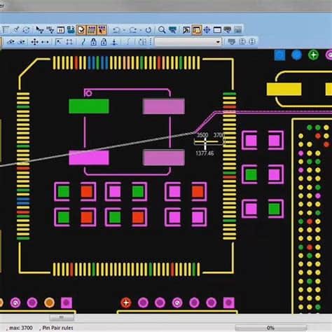
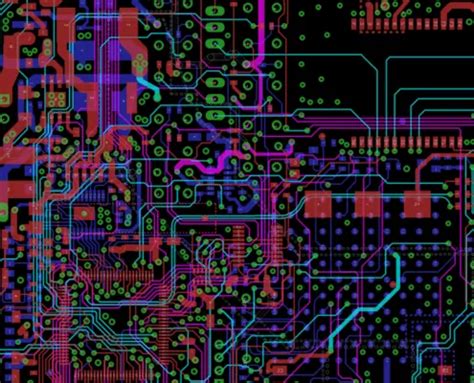
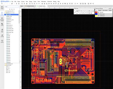
PCB Layout and Routing Techniques
- Partitioning the PCB into functional blocks
- Optimizing component placement for signal integrity and manufacturability
- Routing techniques for high-speed signals and differential pairs
- Implementing proper grounding and shielding strategies
- Adhering to design for manufacturing (DFM) guidelines
Signal Integrity and EMI/EMC Considerations
- Understanding and mitigating signal integrity issues (reflections, crosstalk, etc.)
- Designing for EMI/EMC compliance (proper grounding, filtering, shielding)
- Simulating and analyzing critical signals and interfaces
- Implementing best practices for high-speed PCB design
Thermal Management and Mechanical Design
- Designing for adequate heat dissipation and thermal management
- Selecting appropriate PCB materials and layer stackup
- Integrating mechanical components and enclosures
- Considering environmental factors and reliability requirements

Inter-Board Communication and Interfaces
Choosing Appropriate Communication Protocols
| Protocol | Speed | Distance | Complexity | Cost |
|---|---|---|---|---|
| I2C | Low | Short | Simple | Low |
| SPI | High | Short | Simple | Low |
| UART | Low | Moderate | Simple | Low |
| USB | High | Moderate | Moderate | Moderate |
| Ethernet | High | Long | Complex | High |
| PCIe | Very High | Short | Complex | High |
Designing Robust Connectors and Cables
- Selecting connectors based on signal requirements, durability, and cost
- Ensuring proper shielding and grounding of cables
- Considering mechanical strain relief and cable management
- Adhering to industry standards and specifications
Power Distribution and Grounding Strategies
- Implementing a proper power distribution network (PDN)
- Designing separate power planes for analog and digital circuitry
- Minimizing ground loops and ensuring low-impedance grounding
- Using decoupling capacitors and ferrite beads for noise suppression
Testing, Validation, and Integration
Developing a Comprehensive Test Plan
- Defining test cases and acceptance criteria for each PCB
- Establishing test setups and equipment requirements
- Creating test procedures and documentation
- Allocating resources and timelines for testing activities
Performing Individual PCB Testing
- Visual inspection and continuity tests
- Functional testing and debugging
- Signal integrity and EMI/EMC measurements
- Thermal and environmental stress testing
Integrating and Testing the Complete System
- Verifying inter-board communication and interfaces
- Conducting system-level functional tests
- Measuring overall system performance and power consumption
- Identifying and resolving integration issues
Documenting Test Results and Making Necessary Revisions
- Compiling test reports and data
- Analyzing test results and identifying areas for improvement
- Making necessary revisions to schematic, layout, or component selection
- Updating documentation and design files
Best Practices and Tips for Multi-Board PCB Design
- Start with a clear and well-defined system architecture
- Establish a consistent naming and numbering scheme for components and nets
- Use modular design approaches to simplify integration and testing
- Implement version control and documentation management systems
- Collaborate closely with mechanical and software teams
- Conduct regular design reviews and cross-functional meetings
- Plan for manufacturability, testability, and scalability from the early stages
- Stay updated with the latest industry standards and design tools
Frequently Asked Questions (FAQ)
1. How do I determine the number of PCBs needed for my project?
The number of PCBs required for a project depends on various factors such as functionality, size constraints, power requirements, and modularity. Analyze the system-level block diagram and allocate functions to each PCB based on these factors. It’s essential to strike a balance between the number of PCBs and the complexity of each board.
2. What are the key challenges in designing multiple PCBs for the same project?
Some of the key challenges include ensuring proper communication and interfaces between boards, managing signal integrity and EMI/EMC issues, optimizing power distribution and grounding, and integrating mechanical components. Coordinating tasks and maintaining consistency across multiple PCBs can also be challenging.
3. How can I ensure seamless integration of multiple PCBs?
To ensure seamless integration, start with a well-defined system architecture and establish clear interfaces between boards. Use consistent naming and numbering schemes, and implement modular design approaches. Conduct regular design reviews and cross-functional meetings to identify and resolve integration issues early in the design process.
4. What are some best practices for managing signal integrity in multi-board PCB design?
Some best practices include partitioning the PCB into functional blocks, optimizing component placement, using appropriate routing techniques for high-speed signals, implementing proper grounding and shielding strategies, and simulating and analyzing critical signals. It’s also essential to follow design for manufacturing (DFM) guidelines and industry standards.
5. How can I effectively collaborate with other teams (mechanical, software) in a multi-board PCB design project?
Effective collaboration involves regular communication, clear definition of responsibilities, and sharing of design files and documentation. Establish a common platform for version control and data management. Conduct regular cross-functional meetings to discuss design progress, integration challenges, and potential solutions. Foster a culture of openness and transparency to ensure smooth collaboration.
Conclusion
Designing multiple PCBs for the same project requires careful planning, coordination, and attention to detail. By following best practices and considering key aspects such as system architecture, signal integrity, power distribution, and inter-board communication, designers can create robust and reliable multi-board systems. Effective collaboration, thorough testing, and continuous improvement are essential for successful project execution. As PCB design tools and technologies continue to evolve, staying updated with the latest industry trends and standards is crucial for designing cutting-edge electronic products.
No responses yet