What is PCB Trace to Plane Capacitance?
PCB trace to plane capacitance refers to the parasitic capacitance that exists between a PCB trace and an adjacent power or ground plane. This capacitance is an unintentional but unavoidable consequence of the physical geometry and proximity of conductive elements on a printed circuit board.
Understanding and calculating PCB trace to plane capacitance is important for high-speed digital and RF circuit design. The parasitic capacitance can impact signal integrity, propagation delay, impedance matching, crosstalk, and electromagnetic interference (EMI). By quantifying the capacitance using formulas, PCB designers can optimize the board layout to minimize undesired effects.
Key Factors Affecting PCB Trace to Plane Capacitance
Several factors influence the amount of parasitic capacitance between a PCB trace and plane:
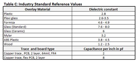
- Dielectric constant (εr): The dielectric constant of the insulating material between the trace and plane. Common PCB materials and their typical dielectric constants are:
| Material | Dielectric Constant (εr) |
|---|---|
| Air | 1.0 |
| FR-4 | 4.2 – 4.5 |
| Rogers RO4003C | 3.38 |
| Rogers RO4350B | 3.48 |
| Isola IS410 | 3.96 |
-
Trace width (w): The width of the PCB trace. Wider traces result in higher capacitance.
-
Trace height (h): The distance between the trace and the reference plane. Smaller heights increase capacitance.
-
Trace length (l): The length of the trace segment running parallel to the plane. Longer traces have greater capacitance.
PCB Trace to Plane Capacitance Formula
The most commonly used formula for calculating the capacitance between a PCB trace and a plane is:
C = ε0 * εr * (w * l) / h
Where:
– C is the capacitance in farads (F)
– ε0 is the permittivity of free space (8.85 × 10^-12 F/m)
– εr is the dielectric constant of the insulating material
– w is the width of the trace in meters (m)
– l is the length of the trace in meters (m)
– h is the distance between the trace and plane in meters (m)
This formula assumes that the trace and plane are parallel, the dielectric material is homogeneous, and fringing effects are negligible. It provides a good approximation for most common PCB geometries.
Example Calculation
Let’s calculate the PCB trace to plane capacitance for the following scenario:
- PCB material: FR-4 (εr = 4.3)
- Trace width (w): 0.2 mm (0.0002 m)
- Trace length (l): 50 mm (0.05 m)
- Distance between trace and plane (h): 0.3 mm (0.0003 m)
Plugging these values into the formula:
C = (8.85 × 10^-12 F/m) * 4.3 * (0.0002 m * 0.05 m) / 0.0003 m
  = 1.27 × 10^-12 F
  = 1.27 pF
The calculated capacitance between the trace and plane in this example is approximately 1.27 picofarads (pF).
Impact of PCB Trace to Plane Capacitance
Signal Integrity and Propagation Delay
PCB trace to plane capacitance can affect signal integrity and propagation delay. The parasitic capacitance forms a low-pass filter with the trace’s resistance and inductance, leading to signal attenuation and dispersion. This effect is more pronounced for high-frequency signals, as the capacitive reactance decreases with increasing frequency.
The increased capacitance also results in a slower signal propagation velocity and longer rise/fall times. The propagation delay (td) due to the trace to plane capacitance can be estimated using the following formula:
td = 0.475 * sqrt(εr) * l * sqrt(C / (w * h))
Where:
– td is the propagation delay in seconds (s)
– εr is the dielectric constant of the insulating material
– l is the length of the trace in meters (m)
– C is the trace to plane capacitance in farads (F)
– w is the width of the trace in meters (m)
– h is the distance between the trace and plane in meters (m)
To minimize the impact on signal integrity and propagation delay, designers should:
- Choose PCB Materials with lower dielectric constants
- Reduce trace lengths when possible
- Increase the distance between traces and planes
- Use appropriate trace widths for the desired characteristic impedance
Crosstalk and EMI
PCB trace to plane capacitance can contribute to crosstalk and electromagnetic interference (EMI) issues. Crosstalk occurs when a signal on one trace couples to another nearby trace through the parasitic capacitance. This unwanted interaction can lead to signal distortion, false triggering, and reduced noise margins.
To mitigate crosstalk, designers should:
- Increase spacing between sensitive traces
- Route critical traces on different layers
- Use guard traces or ground shields between sensitive traces
- Minimize parallel run lengths of adjacent traces
EMI can occur when the parasitic capacitance provides a path for high-frequency noise to couple from traces to planes or vice versa. This noise can radiate from the PCB, causing interference with nearby electronic devices. To reduce EMI, designers should:
- Use proper grounding and power plane design techniques
- Implement decoupling capacitors close to noise sources
- Minimize trace to plane capacitance in sensitive areas
- Consider using EMI shielding or filtering components

Advanced PCB Trace to Plane Capacitance Considerations
Multilayer PCBs
In multilayer PCBs, traces can have different capacitances to planes on various layers. The total trace to plane capacitance is the sum of the individual capacitances to each plane. For example, consider a trace on an inner layer with planes above and below:
Ctotal = Cabove + Cbelow
Where:
– Ctotal is the total trace to plane capacitance
– Cabove is the capacitance between the trace and the plane above
– Cbelow is the capacitance between the trace and the plane below
To accurately calculate the capacitance in multilayer PCBs, designers must consider the stack-up geometry and the presence of power and ground planes on different layers.
Coplanar Waveguides
Coplanar waveguides (CPWs) are a type of transmission line structure used in high-frequency PCB designs. CPWs consist of a center signal trace with ground planes on either side, all on the same layer. The trace to plane capacitance for CPWs can be calculated using the following formula:
C = ε0 * εr * (K(k) / K'(k)) * l
Where:
– C is the capacitance in farads (F)
– ε0 is the permittivity of free space (8.85 × 10^-12 F/m)
– εr is the dielectric constant of the insulating material
– K(k) and K'(k) are complete elliptic integrals of the first kind
– k is the geometric factor, calculated as k = w / (w + 2s)
– w is the width of the center trace in meters (m)
– s is the gap between the center trace and ground planes in meters (m)
– l is the length of the CPW in meters (m)
Designing CPWs with the appropriate trace width, gap, and dielectric material is crucial for achieving the desired characteristic impedance and minimizing parasitic capacitance.
FAQ
1. What is the difference between trace to plane capacitance and trace to trace capacitance?
Trace to plane capacitance is the parasitic capacitance between a PCB trace and an adjacent power or ground plane, while trace to trace capacitance is the parasitic capacitance between two neighboring traces on the same layer or on different layers. Trace to trace capacitance is a primary contributor to crosstalk, while trace to plane capacitance affects signal integrity and EMI.
2. How does the height between a trace and plane affect the capacitance?
The height between a trace and plane is inversely proportional to the capacitance. As the distance between the trace and plane decreases, the capacitance increases. This is because the electric field between the trace and plane is stronger when they are closer together, resulting in a higher charge storage capacity.
3. Can PCB trace to plane capacitance be used intentionally in circuit design?
Yes, PCB trace to plane capacitance can be used intentionally in certain cases. For example, designers can create Controlled Impedance traces by carefully selecting the trace width, height, and dielectric material to achieve a specific capacitance value. This technique is often used in high-frequency and RF circuits to match impedances and minimize reflections.
4. How can I measure PCB trace to plane capacitance in a fabricated board?
PCB trace to plane capacitance can be measured using a Vector Network Analyzer (VNA) or an LCR meter. To measure the capacitance, you need to:
- Identify the trace and plane of interest
- Isolate the trace from other components and traces
- Connect the VNA or LCR meter probes to the trace and plane
- Measure the S-parameters (for VNA) or capacitance (for LCR meter) at the desired frequency range
- Analyze the results and compare them with the calculated values
5. Are there any software tools that can help calculate PCB trace to plane capacitance?
Yes, several PCB design and simulation software packages include tools for calculating trace to plane capacitance. Some popular options are:
- Altium Designer
- Cadence Allegro PCB Designer
- Mentor Graphics HyperLynx
- Polar Instruments Si9000e
- CST Studio Suite
These tools can help designers quickly estimate the parasitic capacitance based on the PCB layout and stack-up, allowing for optimizations early in the design process.
Conclusion
PCB trace to plane capacitance is an essential consideration in high-speed digital and RF circuit design. This parasitic capacitance can significantly impact signal integrity, propagation delay, crosstalk, and EMI. By understanding the factors that influence trace to plane capacitance and using appropriate formulas to calculate its value, PCB designers can make informed decisions to minimize its effects.
Optimizing the PCB layout, choosing suitable materials, and implementing best practices for grounding and shielding can help mitigate the undesired consequences of trace to plane capacitance. As PCB designs continue to push the boundaries of speed and complexity, a solid grasp of this concept will remain crucial for engineers and designers alike.
No responses yet