Introduction to Controlled Impedance
Controlled impedance is a crucial concept in the realm of electronics and Electrical Engineering. It refers to the precise management of the impedance values in electronic circuits, particularly in high-speed digital systems and radio frequency (RF) applications. Maintaining controlled impedance is essential for ensuring Signal integrity, minimizing signal reflections, and optimizing the overall performance of electronic devices.
In this comprehensive article, we will delve into the importance of controlled impedance, exploring its fundamental principles, applications, and the techniques used to achieve it. We will also discuss the challenges associated with controlled impedance and provide insights into best practices for designing and manufacturing electronic systems with controlled impedance requirements.
Understanding Impedance
Before we explore the significance of controlled impedance, let’s briefly review the concept of impedance itself. Impedance is a measure of the opposition that a circuit presents to the flow of alternating current (AC) at a given frequency. It is a complex quantity that consists of both resistance and reactance.
Resistance is the opposition to the flow of current due to the inherent properties of the conducting material, while reactance is the opposition to the flow of current due to the presence of capacitive or inductive elements in the circuit. The combination of resistance and reactance determines the overall impedance of a circuit.
Mathematically, impedance is expressed as a complex number, with the real part representing resistance and the imaginary part representing reactance. The magnitude of impedance is measured in ohms (Ω), and its phase angle indicates the relative contributions of resistance and reactance.
The Importance of Matching Impedance
One of the primary reasons why controlled impedance is crucial in electronic systems is the need for Impedance Matching. When a signal travels from one point to another in a circuit, it encounters various components and interconnects along the way. If the impedance of these components and interconnects is not properly matched, signal reflections can occur.
Signal reflections happen when a portion of the signal energy is reflected back towards the source instead of being transmitted to the intended destination. These reflections can lead to several problems, including:
-
Signal distortion: Reflections can cause the signal waveform to become distorted, leading to errors in data transmission and potentially compromising the functionality of the system.
-
Reduced signal strength: When a significant portion of the signal energy is reflected, the strength of the signal reaching the intended destination is reduced, which can result in poor signal-to-noise ratio and decreased performance.
-
Interference: Reflected signals can interfere with other signals in the system, causing crosstalk and further degrading the overall signal integrity.
To minimize signal reflections and ensure optimal signal transmission, it is essential to match the impedance of the source, the transmission medium (such as traces on a printed circuit board or cables), and the load (the receiving end of the signal). This is where controlled impedance comes into play.

Techniques for Achieving Controlled Impedance
There are several techniques used to achieve controlled impedance in electronic systems. These techniques involve careful design and manufacturing processes to ensure that the impedance of the interconnects and components matches the desired value. Some common techniques include:
-
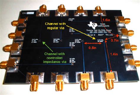
Trace geometry control: The width, thickness, and spacing of the traces on a printed circuit board (PCB) can be precisely controlled to achieve the desired impedance. Wider traces generally have lower impedance, while narrower traces have higher impedance. The thickness of the copper layer and the dielectric material also influence the impedance.
-
Dielectric material selection: The choice of dielectric material, such as the substrate of a PCB or the insulation of a cable, plays a significant role in determining the impedance. Materials with higher dielectric constants result in lower impedance, while materials with lower dielectric constants lead to higher impedance.
-
Termination techniques: Proper termination of transmission lines is essential for preventing signal reflections. Techniques such as Series termination, parallel termination, and differential termination are used to match the impedance at the end of the transmission line to the characteristic impedance of the line itself.
-
Impedance calculation and simulation: Advanced software tools are used to calculate and simulate the impedance of interconnects and components based on their geometric and material properties. These simulations help designers optimize the design for controlled impedance before fabrication.
-
Manufacturing process control: Strict manufacturing process controls are necessary to ensure that the designed impedance values are accurately realized in the final product. This includes precise control over the etching process, plating thickness, and material properties.
Applications of Controlled Impedance
Controlled impedance is critical in a wide range of electronic applications, particularly those involving high-speed digital signals and RF systems. Some notable applications include:
-
High-speed digital interfaces: Controlled impedance is essential for high-speed digital interfaces such as USB, HDMI, PCIe, and Ethernet. These interfaces rely on well-controlled impedance to maintain signal integrity and minimize reflections, ensuring reliable data transmission at high speeds.
-
RF and microwave systems: In RF and microwave applications, controlled impedance is crucial for ensuring efficient power transfer and minimizing signal loss. Impedance matching is necessary for optimizing the performance of antennas, filters, and other RF components.
-
Telecommunications: Controlled impedance is vital in telecommunications systems, including cellular networks, fiber optic communication, and satellite communication. Proper impedance matching is required to maximize signal transmission efficiency and minimize signal distortion.
-
Automotive electronics: With the increasing complexity of automotive electronic systems, controlled impedance has become essential for ensuring reliable communication between various electronic control units (ECUs) and sensors. Controlled impedance helps mitigate signal integrity issues in automotive networks such as CAN, LIN, and FlexRay.
-
Medical devices: Medical devices often involve sensitive analog and digital signals that require controlled impedance for accurate measurement and reliable operation. Examples include electrocardiogram (ECG) machines, patient monitoring systems, and medical imaging equipment.
Challenges in Achieving Controlled Impedance
While controlled impedance is crucial for optimal electronic system performance, achieving it can present several challenges. Some of these challenges include:
-
Manufacturing tolerances: Achieving precise impedance values requires tight manufacturing tolerances. Variations in trace width, thickness, and spacing can lead to deviations from the designed impedance. Ensuring consistent manufacturing processes and quality control measures is essential for maintaining controlled impedance.
-
Material variations: Inconsistencies in the dielectric material properties, such as the dielectric constant and loss tangent, can affect the impedance of the interconnects. Careful material selection and validation are necessary to minimize these variations.
-
Environmental factors: Changes in temperature, humidity, and other environmental conditions can influence the impedance of electronic components and interconnects. Designing for controlled impedance must take these factors into account to ensure robustness and reliability.
-
High-frequency effects: As signal frequencies increase, the impact of parasitic effects, such as capacitance and inductance, becomes more pronounced. Designing for controlled impedance at high frequencies requires advanced modeling and simulation techniques to account for these effects.
-
Cost considerations: Implementing controlled impedance techniques can increase the cost of electronic systems due to the need for specialized materials, precise manufacturing processes, and additional design and testing efforts. Balancing cost and performance requirements is a key challenge in implementing controlled impedance.
Best Practices for Designing with Controlled Impedance
To effectively design electronic systems with controlled impedance, designers should follow these best practices:
-
Define impedance requirements early: Clearly specify the impedance requirements for each part of the system, including the target impedance values, tolerance limits, and frequency range. This information should be communicated to all stakeholders, including designers, manufacturers, and test engineers.
-
Use appropriate design tools: Employ advanced design tools, such as Impedance Calculators and electromagnetic simulation software, to accurately model and simulate the impedance of interconnects and components. These tools help optimize the design for controlled impedance and identify potential issues early in the design process.
-
Collaborate with manufacturers: Work closely with PCB fabricators and component suppliers to ensure that they understand the controlled impedance requirements and can meet the necessary manufacturing tolerances. Provide clear specifications and communicate any special requirements or constraints.
-
Perform thorough testing and validation: Conduct comprehensive testing and validation of the manufactured system to verify that the controlled impedance requirements are met. This may involve impedance measurements, time-domain reflectometry (TDR), and signal integrity analysis. Identify and address any deviations from the specified impedance values.
-
Consider the entire signal path: Controlled impedance should be maintained throughout the entire signal path, including PCB traces, connectors, cables, and components. Ensure that all elements of the signal path are properly designed and matched for impedance.
-
Document and communicate: Clearly document the controlled impedance requirements, design guidelines, and test procedures. Communicate this information to all relevant team members and stakeholders to ensure consistency and adherence to the controlled impedance specifications.
Frequently Asked Questions (FAQ)
-
What is controlled impedance, and why is it important?
Controlled impedance refers to the precise management of impedance values in electronic circuits to ensure optimal signal transmission and minimize reflections. It is important because it helps maintain signal integrity, reduce signal distortion, and optimize the overall performance of electronic systems. -
What are the main techniques used to achieve controlled impedance?
The main techniques used to achieve controlled impedance include trace geometry control, dielectric material selection, termination techniques, impedance calculation and simulation, and manufacturing process control. These techniques involve careful design and manufacturing processes to ensure that the impedance of interconnects and components matches the desired value. -
In what applications is controlled impedance critical?
Controlled impedance is critical in applications involving high-speed digital signals and RF systems, such as high-speed digital interfaces (USB, HDMI, PCIe, Ethernet), RF and microwave systems, telecommunications, automotive electronics, and medical devices. These applications require well-controlled impedance to ensure reliable data transmission, efficient power transfer, and minimize signal distortion. -
What are some challenges in achieving controlled impedance?
Challenges in achieving controlled impedance include manufacturing tolerances, material variations, environmental factors, high-frequency effects, and cost considerations. Ensuring precise impedance values requires tight manufacturing tolerances, careful material selection, and advanced modeling and simulation techniques. Balancing cost and performance requirements is also a key challenge. -
What are some best practices for designing with controlled impedance?
Best practices for designing with controlled impedance include defining impedance requirements early, using appropriate design tools, collaborating with manufacturers, performing thorough testing and validation, considering the entire signal path, and documenting and communicating the requirements and guidelines. Following these practices helps ensure that the controlled impedance specifications are met and the electronic system performs optimally.
Conclusion
Controlled impedance is a fundamental concept in the design and manufacturing of electronic systems, particularly those involving high-speed digital signals and RF applications. By precisely managing the impedance values of interconnects and components, designers can ensure optimal signal transmission, minimize reflections, and maintain signal integrity.
Achieving controlled impedance requires a combination of careful design techniques, advanced modeling and simulation tools, precise manufacturing processes, and thorough testing and validation. Designers must consider factors such as trace geometry, dielectric materials, termination techniques, and manufacturing tolerances to achieve the desired impedance values.
While implementing controlled impedance can present challenges, such as cost considerations and manufacturing variations, following best practices and collaborating closely with manufacturers can help overcome these hurdles. By prioritizing controlled impedance in the design and manufacturing process, electronic systems can achieve higher performance, reliability, and overall quality.
As electronic systems continue to evolve and push the boundaries of speed and complexity, the importance of controlled impedance will only continue to grow. Designers and engineers must stay informed about the latest techniques, tools, and best practices in controlled impedance to keep pace with the ever-increasing demands of modern electronic applications.
| Impedance Range | Typical Applications |
|---|---|
| 25-50 Ω | High-speed digital interfaces (USB, HDMI) |
| 50-75 Ω | RF and microwave systems, telecommunications |
| 90-120 Ω | Differential signaling (Ethernet, PCIe) |
| 100-150 Ω | Single-ended signaling (LVDS, SSTL) |
Table 1: Common impedance ranges and their typical applications
By understanding the principles of controlled impedance, employing appropriate design techniques, and adhering to best practices, designers can create electronic systems that deliver optimal performance, reliability, and signal integrity. As we continue to push the boundaries of electronic innovation, controlled impedance will remain a critical aspect of successful electronic design and manufacturing.
No responses yet