Understanding the Fly Buck Converter Topology
Before we get into the nitty-gritty of PCB layout, let’s briefly review the fly buck converter topology. A fly buck converter, also known as a synchronous buck converter, is a type of DC-DC converter that efficiently steps down a higher input voltage to a lower output voltage. It consists of the following main components:
- High-side MOSFET (Q1)
- Low-side MOSFET (Q2)
- Inductor (L1)
- Input capacitor (Cin)
- Output capacitor (Cout)
The high-side and low-side MOSFETs are switched on and off alternately to control the energy transfer from the input to the output through the inductor. The input and output capacitors help smooth the voltage ripple and provide a stable supply to the load.
Key PCB Layout Considerations
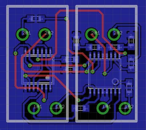
1. Component Placement
Proper component placement is the foundation of a good PCB layout. Follow these guidelines:
- Place the high-side and low-side MOSFETs close together to minimize the high-frequency switching loop area.
- Position the input capacitor as close as possible to the MOSFETs to reduce the input loop inductance.
- Locate the output capacitor near the inductor and load to minimize the output loop inductance.
- Keep the control IC and its associated components away from the high-current switching paths to avoid noise coupling.
2. Power and Ground Planes
Use dedicated power and ground planes to provide low-impedance current paths and minimize voltage drops:
- Create separate power planes for the input voltage (Vin) and output voltage (Vout).
- Use a continuous ground plane to provide a low-impedance return path for the current.
- Connect the ground planes of different circuit sections using multiple vias to reduce impedance.
3. High-Frequency Switching Loop
The high-frequency switching loop is the most critical area in a fly buck converter layout. Minimize the loop area to reduce Parasitic inductance and improve efficiency:
- Route the traces connecting the high-side MOSFET, low-side MOSFET, and input capacitor as short and wide as possible.
- Use multiple vias to connect the components to the power and ground planes.
- Avoid routing any sensitive traces or signals under the switching loop area.
4. Inductor Placement and Routing
The inductor is a key component in a fly buck converter and proper placement and routing are essential:
- Place the inductor away from noise-sensitive components to minimize magnetic field coupling.
- Route the inductor traces as short and wide as possible to reduce resistance and inductance.
- Use a dedicated ground return path for the inductor current to avoid ground loops.
5. Input and Output Capacitors
The input and output capacitors play a crucial role in reducing voltage ripple and providing a stable supply:
- Use low-ESR (Equivalent Series Resistance) capacitors to minimize voltage ripple and power loss.
- Place the capacitors close to the MOSFETs and inductor to minimize loop inductance.
- Use multiple capacitors in parallel to reduce the effective ESR and improve high-frequency performance.
6. Feedback and Control Signals
The feedback and control signals are sensitive to noise and require careful routing:
- Route the feedback trace away from high-current switching paths and noisy components.
- Use a shielded or twisted-pair cable for the feedback signal if it needs to travel a long distance.
- Place a small resistor (e.g., 10Ω) in series with the feedback pin to dampen any ringing or oscillations.
7. Grounding and Shielding
Proper grounding and shielding techniques help reduce EMI and improve Signal integrity:
- Use a single-point ground (star ground) for the sensitive analog and control circuitry.
- Connect the power ground and analog ground at a single point to avoid ground loops.
- Use ground shields or copper pours to isolate sensitive traces from noisy areas.
PCB Layer Stackup
A well-designed PCB layer stackup is essential for good signal integrity and EMI performance. Here’s a recommended 4-layer stackup for a fly buck converter:
| Layer | Purpose |
|---|---|
| Top | Components, signal traces |
| Inner1 | Ground plane |
| Inner2 | Power planes (Vin, Vout) |
| Bottom | Components, signal traces |
This stackup provides a low-impedance ground plane and separate power planes for effective shielding and current distribution.

Thermal Management
Proper thermal management is crucial for the long-term reliability of a fly buck converter. Follow these tips:
- Use a sufficiently large copper area for the MOSFETs and inductor to dissipate heat effectively.
- Place thermal vias under the MOSFETs and inductor to conduct heat to the inner and bottom layers.
- Use a thermal pad or heatsink for the MOSFETs if necessary, especially for high-current applications.
Testing and Verification
After the PCB layout is complete, it’s essential to thoroughly test and verify the fly buck converter’s performance:
- Use a high-bandwidth oscilloscope to measure the switching waveforms and check for any ringing or oscillations.
- Measure the output voltage ripple and ensure it’s within the specified limits.
- Test the converter under various load conditions and temperatures to ensure stability and reliability.
Frequently Asked Questions (FAQ)
1. What is the most critical aspect of a fly buck converter PCB layout?
The most critical aspect is minimizing the high-frequency switching loop area formed by the MOSFETs and input capacitor. This reduces parasitic inductance and improves efficiency.
2. How can I reduce the output voltage ripple?
To reduce the output voltage ripple, use low-ESR output capacitors and place them close to the inductor and load. You can also increase the switching frequency or use a larger inductor value.
3. What is the purpose of the input capacitor?
The input capacitor serves to supply the high-frequency switching current to the MOSFETs and reduce the input voltage ripple. It should be placed as close as possible to the MOSFETs.
4. How do I choose the right inductor for my fly buck converter?
When selecting an inductor, consider the required inductance value, current rating, DC resistance (DCR), and saturation current. The inductor should have a low DCR to minimize power loss and a high enough saturation current to avoid saturation under peak load conditions.
5. What are some common PCB layout mistakes to avoid in a fly buck converter design?
Some common mistakes include:
- Placing the input capacitor too far from the MOSFETs, increasing the switching loop area.
- Routing sensitive traces or signals under the high-current switching path.
- Not using a continuous ground plane or failing to connect ground planes properly.
- Neglecting thermal management, leading to overheating and component failure.
By following the guidelines and best practices outlined in this article, you can create a robust and efficient fly buck converter PCB layout that delivers optimal performance and reliability.
No responses yet