PCB (Printed Circuit Board)
A PCB is a flat board made of insulating material, such as fiberglass or composite epoxy, with conductive pathways printed or etched onto its surface. It is used to mechanically support and electrically connect electronic components using conductive tracks, pads, and other features.
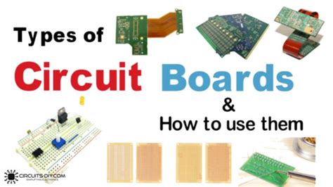
Types of PCBs
- Single-sided PCB: A PCB with conductive traces on only one side of the board.
- Double-sided PCB: A PCB with conductive traces on both sides of the board, connected by vias.
- Multi-layer PCB: A PCB with three or more conductive layers, separated by insulating layers and connected by vias.
- Flexible PCB: A PCB made of flexible materials, such as polyimide, that can be bent or folded to fit into tight spaces or conform to specific shapes.
- Rigid-Flex PCB: A combination of rigid and flexible PCBs, where flexible sections connect multiple rigid sections, allowing for more complex designs and improved reliability.
PCB Design Software
PCB design software is used to create, edit, and analyze PCB layouts. Some popular PCB design software packages include:
- Altium Designer
- KiCad
- Eagle
- OrCAD
- Mentor Graphics PADS
These software tools help designers create schematic diagrams, PCB layouts, and generate manufacturing files such as Gerber and drill files.
PCB components
PCBs are populated with various electronic components that perform specific functions within a circuit. Some common PCB components include:
- Resistors: Components that resist the flow of electric current, used for current limiting, voltage division, and signal conditioning.
- Capacitors: Components that store electric charge, used for filtering, decoupling, and timing applications.
- Inductors: Components that store energy in a magnetic field, used for filtering, power regulation, and signal conditioning.
- Diodes: Components that allow current to flow in only one direction, used for rectification, protection, and switching.
- Transistors: Semiconductor devices used for amplification, switching, and logic operations.
- Integrated Circuits (ICs): Miniaturized electronic circuits that perform specific functions, such as microcontrollers, amplifiers, and sensors.

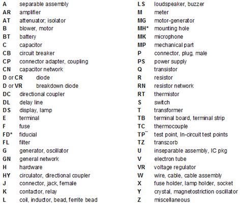
PCB Terminology
A
- Annular Ring: The copper pad surrounding a drilled hole on a PCB, providing electrical connection and mechanical support for components.
- Artwork: The final design files used for PCB fabrication, including copper layers, soldermask, silkscreen, and drill data.
- Aspect Ratio: The ratio of a via’s depth to its diameter, affecting the reliability and manufacturability of the PCB.
B
- BGA (Ball Grid Array): A surface-mount package with a grid of solder balls underneath the component, providing a high-density interconnect solution.
- Blind Via: A via that starts on an outer layer and ends on an inner layer, not passing through the entire board.
- Buried Via: A via that connects two or more inner layers, not visible on the outer layers of the PCB.
C
- Clearance: The minimum distance between two conductive features on a PCB, such as traces, pads, or vias, to prevent unintended electrical connections or short circuits.
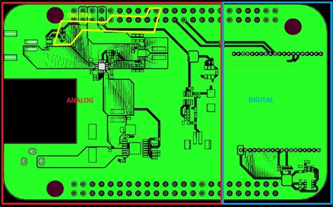
- Controlled Impedance: The precise management of PCB Trace Impedance to maintain signal integrity and minimize reflections, essential for high-speed designs.
- Copper Weight: The thickness of the copper layer on a PCB, typically measured in ounces per square foot (oz/ft²).
D
- DFM (Design for Manufacturability): The practice of designing PCBs to optimize manufacturability, reliability, and cost-effectiveness.
- Drill File: A digital file containing information about the location, size, and type of holes to be drilled in a PCB during fabrication.
E
- ECO (Engineering Change Order): A document that outlines changes to be made to a PCB design after the initial design is complete, often used to address issues or implement improvements.
- EMI (Electromagnetic Interference): Unwanted electromagnetic energy that can disrupt the proper functioning of electronic devices, often requiring shielding or filtering on PCBs.
- ESD (Electrostatic Discharge): The sudden transfer of static electricity between two objects, which can damage electronic components if not properly protected.
F
- Fiducial: A reference mark on a PCB used for aligning and positioning components during assembly.
- Flux: A chemical agent used to remove oxides and promote the flow of solder during the soldering process.
- FR-4: A common PCB substrate material composed of fiberglass and epoxy resin, offering good mechanical and electrical properties.
G
- Gerber File: A standard file format used to describe the artwork of a PCB, including copper layers, soldermask, and silkscreen.
- Ground Plane: A large conductive area on a PCB layer that provides a low-impedance return path for electrical currents and helps reduce EMI.
H
- HDI (High-Density Interconnect): A PCB design technique that uses small vias, fine pitch components, and multiple layers to achieve high component density and improved performance.
- Hole Size: The diameter of a drilled hole in a PCB, typically measured in mils (thousandths of an inch).
I
- Impedance: The total opposition to the flow of alternating current in a circuit, consisting of resistance, capacitance, and inductance.
- IPC (Institute of Printed Circuits): An international standards organization that develops and publishes standards for the PCB industry, covering design, fabrication, and assembly.
J
- JTAG (Joint Test Action Group): A standard interface used for testing, debugging, and programming electronic devices, often implemented on PCBs for boundary scan testing.
K
- Keepout: An area on a PCB where components or traces are not allowed, typically due to mechanical or electrical constraints.
L
- Land Pattern: The arrangement of copper pads and holes on a PCB that corresponds to the pins or contacts of a component, ensuring proper soldering and mechanical stability.
- Layer Stack-up: The arrangement of conductive and insulating layers in a multi-layer PCB, defining the order and spacing of layers.
M
- Microvia: A small via with a diameter less than 6 mils (0.15 mm), used in HDI PCB designs to increase routing density and minimize board size.
- Mil: A unit of measurement equal to one-thousandth of an inch (0.0254 mm), commonly used in PCB design.
N
- Netlists: A text file that describes the connectivity of a PCB, listing the components and the nets (electrical connections) between them.
- Noise: Unwanted electrical signals that can interfere with the proper functioning of a circuit, often requiring filtering or shielding on PCBs.
O
- Outer Layer: The top and bottom layers of a multi-layer PCB, typically used for component placement and routing.
- Oversize Hole: A hole in a PCB that is intentionally larger than the component lead or pin it accommodates, allowing for easier insertion or thermal expansion.
P
- Pad: A conductive area on a PCB used for soldering components or providing electrical connections.
- Panelization: The process of arranging multiple PCB designs on a single panel for fabrication, optimizing material usage and reducing manufacturing costs.
- Plated Through Hole (PTH): A hole in a PCB that is plated with a conductive material, allowing electrical connection between layers.
Q
- QFP (Quad Flat Pack): A surface-mount package with leads extending from all four sides of the component body, commonly used for integrated circuits.
R
- Reflow Soldering: A soldering process where solder paste is applied to the PCB pads, components are placed, and the assembly is heated in an oven to melt the solder and form connections.
- Routing: The process of creating conductive paths (traces) on a PCB to connect components according to the schematic diagram.
S
- Schematic: A graphical representation of an electronic circuit, showing the components and their connections using standardized symbols.
- Silkscreen: A layer on a PCB that contains text, logos, and component outlines, used for identification and assembly guidance.
- SMD (Surface Mount Device): An electronic component designed to be soldered directly onto the surface of a PCB, without requiring through-hole mounting.
- Soldermask: A protective layer applied to a PCB that prevents solder from adhering to unintended areas, while exposing the pads for soldering.
- Stackup: See “Layer Stack-up”.
T
- Thermal Pad: A large conductive area on a PCB designed to dissipate heat from a component, often connected to a ground plane or heatsink.
- Thermocouple: A temperature sensor that consists of two dissimilar metals joined together, producing a voltage proportional to the temperature difference between the junction and the reference point.
- Through-hole: A mounting style where component leads are inserted through holes in the PCB and soldered on the opposite side.
- Trace: A conductive path on a PCB that connects components according to the schematic diagram.
- Trace Width: The width of a conductive trace on a PCB, affecting resistance, current carrying capacity, and impedance.
U
- UL (Underwriters Laboratories): An international safety consulting and certification company that tests and certifies PCBs and electronic components for safety and compliance.
V
- Via: A conductive hole in a PCB that connects traces on different layers, allowing electrical signals to pass through the board.
- Voltage Divider: A simple circuit consisting of two resistors in series, used to produce an output voltage that is a fraction of the input voltage.
W
- Wave Soldering: A soldering process where the PCB is passed over a molten solder wave, allowing the solder to wick into the through-holes and create connections.
X
- X-Out: A marking on a PCB or component indicating that it has failed inspection or testing and should not be used in the final assembly.
Y
- Yield: The percentage of PCBs or components that pass inspection and testing, meeting the required quality standards.
Z
- Z-axis: The vertical axis in a PCB stack-up, perpendicular to the plane of the board, along which components are placed and vias traverse.
PCB Design Guidelines
To ensure optimal performance, manufacturability, and reliability, PCB designers should follow a set of guidelines, such as:
- Maintain proper clearances: Ensure that the minimum clearance between conductive features is maintained to prevent short circuits and unintended connections.
- Use appropriate trace widths: Select trace widths based on the current carrying requirements and impedance constraints of the circuit.
- Follow manufacturer’s recommendations: Adhere to the component manufacturer’s guidelines for land patterns, soldering, and handling to ensure proper functionality and reliability.
- Optimize component placement: Place components in a logical and efficient manner, minimizing trace lengths, reducing crosstalk, and facilitating assembly.
- Consider thermal management: Incorporate thermal management techniques, such as thermal pads, heatsinks, and proper ventilation, to prevent overheating and ensure long-term reliability.
Frequently Asked Questions (FAQ)
- What is the difference between a single-sided and double-sided PCB?
-
A single-sided PCB has conductive traces on only one side of the board, while a double-sided PCB has conductive traces on both sides, connected by vias. Double-sided PCBs offer more design flexibility and higher component density compared to single-sided PCBs.
-
What is the purpose of a soldermask on a PCB?
-
A soldermask is a protective layer applied to a PCB that prevents solder from adhering to unintended areas while exposing the pads for soldering. It helps prevent short circuits, improves the PCB’s appearance, and protects the copper traces from oxidation and damage.
-
What is the difference between a through-hole and surface-mount component?
-
Through-hole components have leads that are inserted through holes in the PCB and soldered on the opposite side, while surface-mount components are soldered directly onto the surface of the PCB without requiring holes. Surface-mount components are generally smaller and allow for higher component density compared to through-hole components.
-
What is a Gerber file, and why is it important in PCB fabrication?
-
A Gerber file is a standard file format used to describe the artwork of a PCB, including copper layers, soldermask, and silkscreen. It contains the necessary information for PCB manufacturers to fabricate the board according to the designer’s specifications. Gerber files are essential for communicating the PCB design to the fabrication house.
-
What is controlled impedance, and why is it important in high-speed PCB designs?
- Controlled impedance is the precise management of PCB trace impedance to maintain signal integrity and minimize reflections. It is essential in high-speed designs to ensure that signals propagate correctly and maintain their shape and timing. Controlled impedance is achieved by carefully selecting trace widths, spacing, and dielectric materials based on the desired impedance values.
In conclusion, understanding PCB terminology is essential for effective communication and collaboration among PCB designers, manufacturers, and assemblers. By familiarizing yourself with the terms and concepts outlined in this comprehensive PCB glossary, you’ll be better equipped to navigate the complex world of PCB design and bring your electronic projects to life.
No responses yet