What is a PCB Layer Stack?
A printed circuit board (PCB) layer stack refers to the arrangement and configuration of the various layers that make up a PCB. The layer stack determines the electrical, mechanical, and thermal properties of the PCB, making it a critical aspect of PCB design. By carefully selecting the number, type, and order of layers in the stack, designers can optimize the performance, reliability, and manufacturability of their PCBs.
Key Components of a PCB Layer Stack
A typical PCB layer stack consists of the following components:
-
Copper layers: These are the conductive layers that carry electrical signals and power throughout the PCB. The number of copper layers can vary from one (single-sided) to multiple (multi-layer) depending on the complexity of the circuit.
-
Dielectric layers: Also known as insulating layers, these are non-conductive materials that separate the copper layers and provide electrical isolation. The most common dielectric materials are FR-4, Rogers, and polyimide.
-
Solder mask: This is a protective coating applied to the outer layers of the PCB to prevent oxidation and improve solderability. It also helps to prevent solder bridges and short circuits during assembly.
-
Silkscreen: This is a printed layer on top of the solder mask that provides text, logos, and other markings for component placement and identification.
Why is the PCB Layer Stack Important?
The PCB layer stack plays a crucial role in determining the performance and reliability of the finished circuit board. Here are some of the key reasons why the layer stack is so important:
Signal Integrity
The layer stack can have a significant impact on signal integrity, particularly for high-speed and high-frequency designs. Factors such as the dielectric constant, thickness, and spacing of the layers can affect the propagation of signals through the board, leading to issues such as crosstalk, reflections, and EMI.
Power Integrity
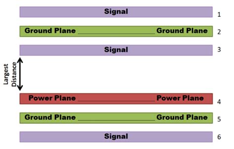
The layer stack also influences power integrity by determining the resistance and inductance of the power distribution network. Proper placement and sizing of power and ground planes can minimize voltage drops, reduce noise, and improve overall power quality.
Thermal Management
The choice of materials and the arrangement of layers in the stack can affect the thermal performance of the PCB. For example, using high-thermal-conductivity dielectrics or adding dedicated thermal layers can help to dissipate heat more effectively, preventing component overheating and failure.
Mechanical Strength
The layer stack contributes to the mechanical strength and stability of the PCB. Thicker boards with more layers tend to be more rigid and resistant to warping and vibration. However, this must be balanced against the increased cost and weight of the board.
Common PCB Layer Stack Configurations
There are several standard layer stack configurations that are widely used in PCB design. The choice of configuration depends on the specific requirements of the application, such as the number of components, the signal and power requirements, and the operating environment.
Single-Layer PCBs
Single-layer PCBs, also known as single-sided PCBs, have conductive copper on only one side of the board. They are the simplest and most economical type of PCB, but they are limited in terms of circuit complexity and density.
| Layer | Material | Thickness (mm) |
|---|---|---|
| Top | Copper | 0.035 |
| Core | FR-4 | 1.6 |
Double-Layer PCBs
Double-layer PCBs have copper on both sides of the board, allowing for more complex circuits and higher component density. They are the most common type of PCB for moderate-complexity applications.
| Layer | Material | Thickness (mm) |
|---|---|---|
| Top | Copper | 0.035 |
| Core | FR-4 | 1.6 |
| Bottom | Copper | 0.035 |
Multi-Layer PCBs
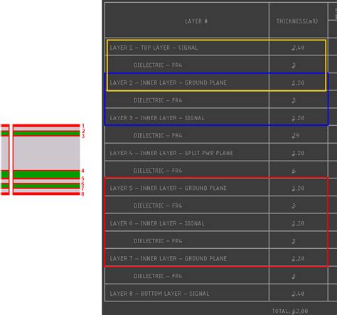
Multi-layer PCBs have three or more copper layers, separated by dielectric materials. They offer the highest level of circuit complexity and density, but they are also the most expensive to manufacture. The number of layers can range from four to over twenty, depending on the application.
| Layer | Material | Thickness (mm) |
|---|---|---|
| Top | Copper | 0.035 |
| Prepreg | FR-4 | 0.2 |
| Inner 1 | Copper | 0.035 |
| Core | FR-4 | 1.2 |
| Inner 2 | Copper | 0.035 |
| Prepreg | FR-4 | 0.2 |
| Bottom | Copper | 0.035 |
4-Layer PCB Stack Example
Here is an example of a typical 4-layer PCB stack:
| Layer | Material | Thickness (mm) |
|---|---|---|
| Top | Copper | 0.035 |
| Prepreg | FR-4 | 0.2 |
| Inner 1 | Copper | 0.035 |
| Core | FR-4 | 1.2 |
| Inner 2 | Copper | 0.035 |
| Prepreg | FR-4 | 0.2 |
| Bottom | Copper | 0.035 |
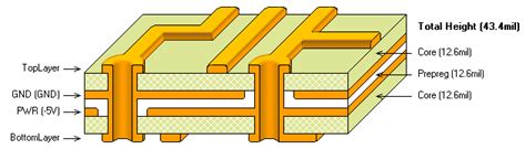
In this configuration, the top and bottom layers are used for component placement and routing, while the inner layers are typically used for power and ground planes. The prepreg layers provide insulation and bonding between the core and the outer layers.
6-Layer PCB Stack Example
For more complex designs, a 6-layer PCB stack might be used:
| Layer | Material | Thickness (mm) |
|---|---|---|
| Top | Copper | 0.035 |
| Prepreg | FR-4 | 0.2 |
| Inner 1 | Copper | 0.035 |
| Core | FR-4 | 1.2 |
| Inner 2 | Copper | 0.035 |
| Prepreg | FR-4 | 0.2 |
| Inner 3 | Copper | 0.035 |
| Core | FR-4 | 1.2 |
| Inner 4 | Copper | 0.035 |
| Prepreg | FR-4 | 0.2 |
| Bottom | Copper | 0.035 |
In this case, the additional inner layers can be used for signal routing, power distribution, or shielding, depending on the specific requirements of the design.

Choosing the Right PCB Layer Stack
Selecting the appropriate PCB layer stack for a given application involves considering several factors, including:
-
Circuit complexity: More complex circuits with a higher component count and greater routing density will require more layers to accommodate all the necessary connections.
-
Signal integrity: High-speed and high-frequency designs may require specific layer arrangements and materials to minimize signal distortion and interference.
-
Power requirements: The number and placement of power and ground layers will depend on the power distribution needs of the circuit.
-
Thermal management: Applications with high heat dissipation requirements may benefit from the use of thermal layers or high-thermal-conductivity materials in the stack.
-
Manufacturing constraints: The choice of layer stack must also consider the capabilities and limitations of the PCB manufacturing process, such as minimum layer thickness, aspect ratios, and material availability.
Best Practices for PCB Layer Stack Design
To ensure optimal performance and manufacturability of your PCB, follow these best practices when designing your layer stack:
-
Use a symmetrical stack: Whenever possible, design your layer stack to be symmetrical about the center layer. This helps to minimize warping and stress on the board during manufacturing and assembly.
-
Minimize layer count: Use the minimum number of layers necessary to achieve the required functionality and performance. Adding unnecessary layers increases cost and complexity.
-
Follow manufacturer guidelines: Consult with your PCB manufacturer to ensure that your layer stack design is compatible with their manufacturing processes and capabilities.
-
Use appropriate materials: Select dielectric materials with the appropriate electrical, thermal, and mechanical properties for your application. Consider factors such as dielectric constant, loss tangent, thermal conductivity, and glass transition temperature.
-
Plan for signal integrity: Use appropriate layer spacing, trace widths, and impedance control techniques to maintain signal integrity throughout the board. Consider the use of dedicated signal layers, ground planes, and shielding layers as needed.
FAQ
1. What is the most common dielectric material used in PCB layer stacks?
FR-4 is the most widely used dielectric material in PCB manufacturing. It is a composite material made of woven fiberglass cloth impregnated with an epoxy resin. FR-4 offers a good balance of electrical, mechanical, and thermal properties at a relatively low cost.
2. How does the number of layers in a PCB stack affect its cost?
In general, the cost of a PCB increases with the number of layers in the stack. This is because each additional layer requires more materials, processing steps, and manufacturing time. However, the cost increase is not linear, as there are certain fixed costs associated with PCB fabrication regardless of the number of layers.
3. What is the purpose of ground planes in a PCB layer stack?
Ground planes serve several important functions in a PCB layer stack. They provide a low-impedance return path for currents, helping to reduce electromagnetic interference (EMI) and maintain signal integrity. They also shield sensitive signals from external noise sources and help to distribute heat more evenly across the board.
4. Can I mix different dielectric materials in the same PCB layer stack?
Yes, it is possible to use different dielectric materials in the same PCB layer stack. This is often done to optimize the electrical, thermal, or mechanical properties of the board for specific applications. For example, a high-speed design might use a low-loss material like Rogers for the critical signal layers, while using FR-4 for the less-sensitive layers to reduce cost.
5. How do I determine the optimal layer stack for my PCB design?
Determining the optimal layer stack for a PCB design requires careful consideration of the specific requirements and constraints of the application. Factors to consider include the circuit complexity, signal integrity, power distribution, thermal management, and manufacturing capabilities. It is recommended to work closely with your PCB manufacturer and use simulation tools to evaluate different layer stack options and select the best configuration for your design.
Conclusion
The PCB layer stack is a critical aspect of PCB design that directly impacts the performance, reliability, and manufacturability of the final product. By understanding the key components and configurations of PCB layer stacks, and following best practices for design and material selection, you can optimize your PCB design for your specific application requirements. Whether you are working on a simple single-layer board or a complex multi-layer design, taking the time to carefully plan and optimize your layer stack will pay off in terms of improved functionality, reliability, and cost-effectiveness.
No responses yet