What is Trace Impedance and Why Does it Matter?
Trace impedance, also known as characteristic impedance, refers to the resistance to the flow of electrical signals in a PCB trace or transmission line. It is a critical parameter in high-speed PCB design as it affects signal integrity, power integrity, and electromagnetic compatibility (EMC) of the board.
Maintaining a consistent and matched trace impedance is essential for several reasons:
- Signal Integrity: Mismatched impedances can cause reflections, ringing, and distortions in the signal waveform, leading to data corruption, jitter, and bit errors.
- Power Integrity: Impedance discontinuities can cause voltage drops, ground bounces, and power supply noise, affecting the performance and reliability of the circuit.
- EMC: Uncontrolled impedance can result in increased electromagnetic emissions, crosstalk, and susceptibility to external interference, making it difficult to meet EMC regulations.
Therefore, designers must carefully calculate and control the trace impedance to ensure proper functioning and compliance of the PCB.
Factors Affecting Trace Impedance
Several factors influence the characteristic impedance of a PCB trace:
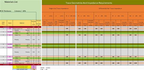
- Trace geometry: The width, thickness, and cross-sectional shape of the trace determine its resistance and capacitance per unit length.
- Dielectric material: The permittivity (Ɛr) and thickness of the dielectric material (substrate) between the trace and the reference plane affect the capacitance.
- Reference plane: The proximity and size of the ground or power plane beneath the trace influence the inductance and capacitance.
- Frequency: The impedance varies with frequency due to the skin effect and dielectric losses, especially at high frequencies.
- Manufacturing tolerances: Variations in trace width, dielectric thickness, and copper roughness during PCB fabrication can cause impedance deviations.
Trace Impedance Calculation Methods
There are several methods to calculate the characteristic impedance of a PCB trace, depending on the trace geometry and dielectric configuration. Some common methods include:
1. Microstrip Trace Impedance
A microstrip is a trace on the outer layer of a PCB, with a reference plane on the opposite side of the dielectric. The characteristic impedance of a microstrip trace can be calculated using the following formula:
Z₀ = (87 / √(Ɛr + 1.41)) * ln(5.98 * h / (0.8 * w + t))
Where:
– Z₀ is the characteristic impedance in ohms (Ω)
– Ɛr is the relative permittivity of the dielectric material
– h is the dielectric thickness in mils (1 mil = 0.001 inch)
– w is the trace width in mils
– t is the trace thickness (copper thickness) in mils
For example, let’s calculate the impedance of a microstrip trace with the following parameters:
– Ɛr = 4.5 (FR-4 substrate)
– h = 5 mils
– w = 10 mils
– t = 1.4 mils (1 oz copper)
Plugging these values into the formula:
Z₀ = (87 / √(4.5 + 1.41)) * ln(5.98 * 5 / (0.8 * 10 + 1.4))
= (87 / √5.91) * ln(29.9 / 9.4)
= 35.8 * ln(3.18)
= 35.8 * 1.16
= 41.5 Ω
Therefore, the microstrip trace has a characteristic impedance of approximately 41.5 ohms.
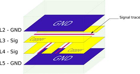
2. Stripline Trace Impedance
A stripline is a trace embedded between two dielectric layers, with reference planes on both sides. The characteristic impedance of a stripline trace can be calculated using the following formula:
Z₀ = (60 / √Ɛr) * ln(4 * h / (0.67 * (0.8 * w + t)))
Where:
– Z₀ is the characteristic impedance in ohms (Ω)
– Ɛr is the relative permittivity of the dielectric material
– h is the dielectric thickness in mils (distance from trace to reference plane)
– w is the trace width in mils
– t is the trace thickness (copper thickness) in mils
For example, let’s calculate the impedance of a stripline trace with the following parameters:
– Ɛr = 4.5 (FR-4 substrate)
– h = 10 mils (5 mils on each side)
– w = 8 mils
– t = 1.4 mils (1 oz copper)
Plugging these values into the formula:
Z₀ = (60 / √4.5) * ln(4 * 10 / (0.67 * (0.8 * 8 + 1.4)))
= (60 / 2.12) * ln(40 / (0.67 * 7.8))
= 28.3 * ln(40 / 5.23)
= 28.3 * ln(7.65)
= 28.3 * 2.03
= 57.5 Ω
Therefore, the stripline trace has a characteristic impedance of approximately 57.5 ohms.
3. Coplanar Waveguide (CPW) Trace Impedance
A coplanar waveguide is a trace on the outer layer of a PCB, with ground planes on either side of the trace. The characteristic impedance of a CPW trace can be calculated using the following formula:
Z₀ = (30π / √Ɛeff) * K(k’) / K(k)
Where:
– Z₀ is the characteristic impedance in ohms (Ω)
– Ɛeff is the effective dielectric constant
– K(k) and K(k’) are complete elliptic integrals of the first kind
– k = w / (w + 2s)
– k’ = √(1 – k²)
– w is the trace width in mils
– s is the gap width between trace and ground plane in mils
The calculation of CPW impedance involves complex mathematical functions and is usually done using specialized software or online calculators.

Impedance Control in PCB Design
To achieve the desired trace impedance in a PCB design, designers can follow these steps:
- Determine the target impedance: Based on the application, signaling standard, and system requirements, decide on the target impedance value (e.g., 50 Ω, 75 Ω, 100 Ω).
- Choose the appropriate dielectric material: Select a substrate material with a suitable dielectric constant (Ɛr) and loss tangent (tan δ) for the desired frequency range and impedance.
- Calculate the trace geometry: Use the impedance calculation formulas or software tools to determine the trace width, thickness, and spacing that yield the target impedance.
- Adjust the stackup: If needed, modify the dielectric thickness, number of layers, and reference plane configuration to optimize the impedance and manufacturability.
- Route the traces: During PCB layout, route the traces according to the calculated geometry and follow good design practices, such as avoiding sharp bends, maintaining consistent spacing, and minimizing discontinuities.
- Perform impedance simulation: Use electromagnetic (EM) simulation tools to analyze the impedance of critical traces and identify any discontinuities or mismatches.
- Specify impedance requirements: Communicate the impedance specifications and tolerances to the PCB fabricator, including the target impedance, dielectric material, and copper weight.
- Verify the impedance: After PCB fabrication, perform impedance testing using a time-domain reflectometer (TDR) or other methods to ensure that the actual impedance matches the designed value within acceptable tolerances.
Impedance-Controlled PCB Manufacturing
To manufacture PCBs with controlled impedance, fabricators use specialized processes and equipment, such as:
- Precise etching: High-quality photolithography and etching techniques are used to achieve accurate trace widths and spacings.
- Controlled dielectric thickness: The dielectric material is carefully pressed or laminated to maintain a consistent thickness across the board.
- Copper surface treatment: The copper surface is treated to minimize roughness and variations in thickness, which can affect the impedance.
- Impedance testing: TDR or other impedance measurement methods are used to verify the impedance of each production panel or batch.
Impedance-controlled PCBs may have a higher cost and longer lead time compared to standard PCBs due to the additional processing and testing requirements.
Impedance Calculator Tools and Resources
Several online tools and resources are available to help designers calculate and optimize trace impedance:
- Online impedance calculators:
- EEWeb PCB Impedance Calculator
- Microstrip Impedance Calculator
- Stripline Impedance Calculator
- Saturn PCB Toolkit
- PCB design software with integrated impedance calculators:
- Altium Designer
- Cadence Allegro PCB Designer
- Mentor Graphics PADS
- KiCad EDA
- Technical papers and application notes:
- Impedance Matching and the Smith Chart: The Fundamentals
- High-Speed PCB Layout Techniques
- Signal Integrity: Tips, Tricks, and Techniques
- Textbooks and reference guides:
- “High-Speed Digital Design: A Handbook of Black Magic” by Howard Johnson and Martin Graham
- “Signal and Power Integrity – Simplified” by Eric Bogatin
- “High-Speed Signal Propagation: Advanced Black Magic” by Howard Johnson and Martin Graham
By utilizing these tools and resources, designers can effectively calculate and control trace impedance for optimal signal integrity and EMC in their PCB designs.
Frequently Asked Questions (FAQ)
1. What is the most common impedance value used in PCB design?
The most common impedance value used in PCB design is 50 ohms. This value is widely used in RF and high-speed digital systems because it provides a good balance between power handling, signal integrity, and compatibility with standard connectors and components. Other common impedance values include 75 ohms (used in video and cable applications) and 100 ohms (used in differential signaling, such as Ethernet and USB).
2. What happens if the trace impedance is not matched to the source and load impedance?
If the trace impedance is not matched to the source and load impedance, several issues can occur:
- Reflections: When a signal encounters an impedance mismatch, a portion of the signal energy is reflected back towards the source, causing signal distortion and ringing.
- Signal attenuation: Impedance mismatches can cause the signal to be attenuated or lost, reducing the signal strength and integrity.
- Standing waves: Reflections can combine with the original signal to create standing waves, leading to voltage and current variations along the trace.
- Crosstalk: Mismatched impedances can increase the coupling of signals between adjacent traces, causing crosstalk and noise.
- EMI: Uncontrolled impedance can result in increased electromagnetic emissions, making it difficult to meet EMC regulations.
To avoid these issues, it is crucial to design traces with a characteristic impedance that matches the source and load impedances and to minimize impedance discontinuities along the signal path.
3. What is the effect of increasing the dielectric thickness on trace impedance?
Increasing the dielectric thickness (h) of a PCB substrate will increase the characteristic impedance of a trace. This can be seen from the impedance calculation formulas for microstrip and stripline traces:
- Microstrip: Z₀ ∝ ln(h)
- Stripline: Z₀ ∝ ln(h)
As the dielectric thickness increases, the natural logarithm (ln) of the thickness also increases, resulting in a higher impedance value. This is because a thicker dielectric reduces the capacitance between the trace and the reference plane, which is inversely proportional to the impedance.
Designers can use this relationship to adjust the impedance by changing the dielectric thickness, along with other parameters such as trace width and spacing. However, increasing the dielectric thickness may also impact other aspects of the PCB design, such as the overall thickness, layer count, and manufacturing cost.
4. Can trace impedance be measured after PCB fabrication?
Yes, trace impedance can be measured after PCB fabrication using various methods, such as:
- Time-Domain Reflectometry (TDR): TDR is the most common method for measuring trace impedance. It involves sending a fast-rise-time pulse along the trace and analyzing the reflections caused by impedance discontinuities. The magnitude and timing of the reflections provide information about the impedance profile along the trace.
- Time-Domain Transmission (TDT): TDT is similar to TDR but measures the transmitted signal instead of reflections. It requires access to both ends of the trace and is useful for characterizing the insertion loss and propagation delay of the trace.
- Vector Network Analyzer (VNA): A VNA measures the scattering parameters (S-parameters) of a trace over a wide frequency range. From the S-parameters, the characteristic impedance and other transmission line properties can be derived.
- Impedance Test Coupons: PCB fabricators often include impedance test coupons on the production panel, which are specially designed traces with known geometry and spacing. By measuring the impedance of these coupons using TDR or other methods, the fabricator can verify that the actual impedance matches the specified value within acceptable tolerances.
Measuring trace impedance after fabrication is an essential part of quality control and ensures that the PCB meets the designed specifications for signal integrity and performance.
5. What are some best practices for designing impedance-controlled PCBs?
When designing impedance-controlled PCBs, consider the following best practices:
- Define the target impedance early in the design process and communicate it clearly to all stakeholders, including the PCB fabricator.
- Choose a suitable dielectric material with a consistent dielectric constant (Ɛr) and low loss tangent (tan δ) for the desired frequency range and impedance.
- Use a symmetric stackup with dedicated reference planes for each signal layer to minimize crosstalk and impedance variations.
- Calculate the trace geometry (width, thickness, and spacing) based on the target impedance and stackup using accurate formulas or simulation tools.
- Route traces with a consistent geometry and avoid abrupt changes in width or direction, which can cause impedance discontinuities.
- Maintain a continuous reference plane beneath the trace and provide sufficient ground vias to minimize inductance and ensure a low-impedance return path.
- Keep high-speed traces away from board edges, connectors, and other potential sources of discontinuities or reflections.
- Simulate the impedance of critical traces using electromagnetic (EM) solvers to identify and resolve any issues before fabrication.
- Specify the impedance requirements and tolerances in the PCB fabrication drawings and work closely with the fabricator to ensure they are met.
- Perform post-fabrication impedance testing using TDR or other methods to verify that the actual impedance matches the designed value within acceptable tolerances.
By following these best practices and carefully controlling the trace impedance throughout the design and manufacturing process, designers can ensure reliable and high-performance PCBs for their applications.
No responses yet