Introduction to PCB antennas
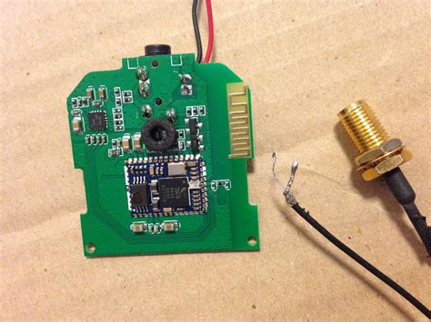
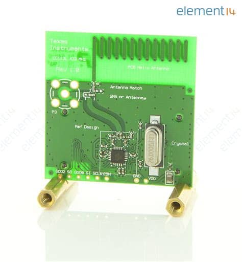
A PCB (printed circuit board) antenna is a key component in many modern wireless devices used for receiving and transmitting radio frequency (RF) signals. PCB antennas are favored for their compact size, low cost, ease of integration, and good performance. They can be manufactured directly on a device’s PCB using standard etching processes.
PCB antennas come in various types and sizes optimized for different frequencies, bandwidths, and applications. Common types include microstrip patch antennas, planar inverted-F antennas (PIFAs), monopole antennas, and dipole antennas. They are widely used in smartphones, tablets, laptops, smart home devices, wearables, medical devices, and IoT sensors.
Advantages of PCB Antennas
- Small size allows integration into compact devices
- Low cost to manufacture using standard PCB fabrication
- Decent performance with proper design
- Support different frequencies and bandwidths
- Durable with no moving parts
- Easy to integrate with other PCB components
How PCB Antennas Work
A PCB antenna converts between electrical signals on the PCB and electromagnetic waves that propagate through the air. They typically consist of copper traces etched onto the PCB substrate in a specific pattern that resonates at the desired frequency. The size, shape and pattern of the traces determines the antenna’s properties.
Transmitting
When transmitting, an oscillating electrical signal from the device’s transmitter circuit is fed to the antenna traces. This creates an oscillating electric field between the traces and a corresponding magnetic field around them. The changing fields radiate away from the antenna as an electromagnetic wave at the signal frequency.
Receiving
The receiving process is the reverse. An incoming electromagnetic wave from a distant transmitter induces a tiny oscillating voltage in the receiving antenna’s traces. This signal is amplified and demodulated by the device’s receiver circuit to extract the transmitted data.
Types of PCB Antennas
There are several common types of PCB antennas, each with its own characteristics:
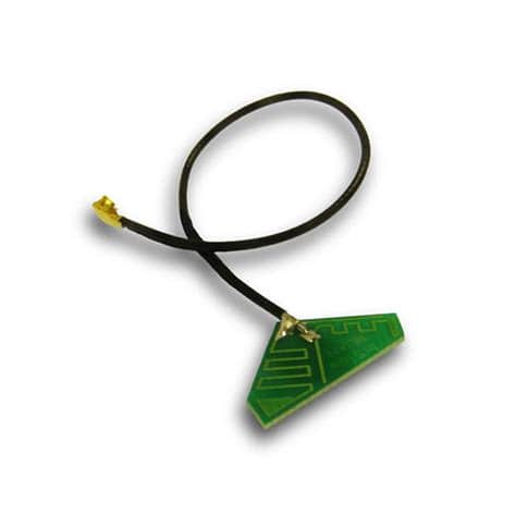
Microstrip Patch Antenna
Microstrip patch antennas consist of a flat rectangular area of copper trace separated from a larger ground plane on the opposite side of the PCB by the board substrate. The patch dimensions are roughly half the wavelength of the resonant frequency.
Advantages:
– Low profile and lightweight
– Easy to fabricate and integrate
– Supports linear and circular polarization
– Moderate bandwidth (few percent of center frequency)
Disadvantages:
– Somewhat narrow bandwidth
– Lower gain compared to some other types
– Efficiency reduced by dielectric losses in PCB substrate
Typical applications:
– GPS receivers
– Wi-Fi and Bluetooth devices
– Satellite links
– Medical implants
– Wireless sensor networks
Planar Inverted-F Antenna (PIFA)
PIFAs are similar to patch antennas but have a shorting pin or wall that connects the top trace element to the ground plane. The shorting pin allows the antenna size to be reduced by half compared to a patch antenna.
Advantages:
– More compact than patch antennas
– Moderate to high gain
– Omnidirectional radiation pattern
– Good efficiency
Disadvantages:
– More complex to design and tune
– Polarization limited to linear
– Bandwidth narrower than patch antennas
Typical applications:
– Cellular phones and smartphones
– Tablets and laptops
– Wearable devices
– Asset tracking tags
Monopole Antenna
A monopole PCB antenna is a straight line of copper trace extending from the transmitter/receiver circuit. The simplest kind is a quarter-wavelength long and mounted perpendicular to a ground plane. Variations include the inverted-L and inverted-F which have a horizontal section.
Advantages:
– Very simple design and easy to fabricate
– Compact size, can be coiled to reduce footprint
– Omnidirectional radiation pattern
– Wideband operation possible
Disadvantages:
– Typically narrowband without wideband techniques
– Requires a large ground plane for good efficiency
– Efficiency limited by resistive losses in trace
Typical applications:
– Cordless phones
– Garage door openers
– Wireless keyboards and mice
– Remote controlled toys
Dipole Antenna
A dipole is a balanced antenna with equal trace arms extending in opposite directions from the feed point. Each arm is a quarter wavelength long, for a total length of a half wavelength. Dipoles can be printed on a PCB substrate or made from stiff wire soldered to the PCB.
Advantages:
– Simple design and easy impedance matching
– Wider bandwidth than monopoles
– Omnidirectional radiation perpendicular to axis
– Higher efficiency possible with thicker wire arms
Disadvantages:
– Needs a balun circuit for interface to unbalanced circuits
– Size can be prohibitive at lower frequencies
– Not as compact as PIFAs or patches
– Efficiency limited by thin PCB traces
Typical applications:
– FM radios and TV receivers
– Wireless microphones
– Remote controls
– Wireless sensors
– RFID tags

PCB antenna design Considerations
Properly designing a PCB antenna is critical for good performance in the final device. There are several key considerations:
Frequency and Bandwidth
The antenna must be designed for the desired operating frequency and have sufficient bandwidth to cover the device’s communication channels. The specific frequency band(s) will depend on the wireless standard being used, such as:
| Wireless Standard | Frequency Bands |
|---|---|
| Bluetooth | 2.4 – 2.485 GHz |
| Wi-Fi (802.11b/g/n) | 2.4 – 2.497 GHz |
| Wi-Fi (802.11a/h/j/n/ac) | 4.915 – 5.825 GHz |
| GPS L1 | 1.563 – 1.587 GHz |
| Cellular 4G LTE | Multiple bands 0.7 – 2.7 GHz |
| 5G NR FR1 | Multiple bands 0.41 – 7.125 GHz |
| 5G NR FR2 | 24.25 – 52.6 GHz |
The antenna’s dimensions must be tuned to resonate at the chosen frequency. Bandwidth can be increased using thicker substrates, proximity fed patches, and other broadbanding techniques.
Radiation Pattern
The radiation pattern is a plot of the antenna’s far-field radiation strength vs. angle. Most antennas are designed to radiate equally in all directions perpendicular to the PCB (omnidirectional pattern). Directional antennas are sometimes used to focus energy in a particular direction. The pattern is affected by the ground plane size and proximity to other components.
Gain and Efficiency
Antenna gain is a measure of how well it converts input power into radiated electromagnetic waves in a particular direction. Gain is limited by the antenna’s electrical size and the efficiency. Efficiency is reduced by resistive losses (trace resistance, dielectric losses) and mismatch losses. Using lower loss PCB laminates like PTFE can increase efficiency.
Size and Form Factor
The antenna must fit within the allotted space in the device enclosure which sets an upper limit on its electrical size. Meandering the traces, folding the geometry (PIFA) and dielectric loading are common miniaturization techniques. However, reducing size can adversely impact gain, efficiency and bandwidth.
Integration and Placement
Antennas should be placed on the PCB to minimize interference from other components like displays, batteries, and digital circuits. Sufficient clearance from the PCB edge and enclosure walls is needed to reduce detuning. Some designs wrap the antenna around the corner or edge of the PCB for a more omni-directional pattern.
Impedance Matching
The impedance looking into the antenna terminals must be matched to the transmitter and receiver impedance (typically 50 ohms) to maximize power transfer and minimize reflections. Impedance can be adjusted by changing the feed location, adding matching stubs/networks or using multi-resonant elements.
Testing and Measurement
Once designed and fabricated, a PCB antenna should be tested and measured to verify it meets the performance requirements. Common tests include:
Return Loss (S11)
This measures how much of the RF energy sent to the antenna is reflected back due to impedance mismatch. It is measured using a vector network analyzer (VNA). A good antenna typically has a return loss better than 10 dB (VSWR < 2) over its operating band.
Gain and Efficiency
Gain and efficiency can be measured using an anechoic chamber or over-the-air test range. The antenna is mounted on a rotating positioner and its radiated power is measured at various angles. The data is used to create 2D or 3D radiation pattern plots. Gain is typically reported in units of dBi (decibels relative to an ideal isotropic radiator).
Polarization
The antenna’s polarization (orientation of the E-field) can be linear (vertical or horizontal), circular (left or right hand) or elliptical. It is measured with a linearly polarized test antenna rotated through different angles. Polarization match between transmit and receive antennas impacts the link budget.
Radiation Hazard
Testing may be required to ensure the device complies with human RF exposure limits set by regulatory agencies like the FCC or ICNIRP. The specific absorption rate (SAR) is measured using standardized phantoms and body models.
Future Trends
5G and mmWave
The rollout of 5G cellular networks is driving development of new PCB antennas operating at much higher frequencies (above 24 GHz). At these millimeter wave frequencies, the antennas can be much smaller but must deal with higher losses and propagation challenges. Phased array antennas with many elements are used for beamforming.
Wireless IoT
The growth of wireless IoT devices is creating demand for low cost, compact, and efficient antennas. Many IoT devices operate in the sub-1 GHz bands for longer range and better building penetration. Printed PCB antennas can meet the cost and size requirements. Dual-band antennas covering both sub-1 GHz and 2.4 GHz are used in some cases.
Wearables
Antennas for wearable devices must be very compact and able to operate near the human body. Flexible PCB antennas that can conform to curved surfaces are being developed. The antenna must also be insensitive to detuning caused by the body or clothing.
Vehicle Connectivity
Modern vehicles incorporate many wireless functions like Bluetooth, Wi-Fi, cellular, and GPS. PCB antennas are used for some of these, while others use external “shark fin” antennas. The trend is towards hidden and integrated antennas for aesthetics. 5G mmWave will enable new applications like V2X Communication.
FAQ
What is the best type of PCB antenna?
There is no one “best” type as the choice depends on the specific application, operating frequency, bandwidth, size constraints, and cost targets. PIFAs and patches are common for their compact size. Monopoles and dipoles offer simplicity. In general, larger antennas are more efficient but take up more space.
How do I choose the right PCB material for an antenna?
The best PCB material depends on the frequency, required bandwidth, and efficiency. FR-4 is commonly used for low cost antennas up to a few GHz. Higher frequency antennas often use PTFE laminates like Rogers Duroid which have lower dielectric loss. Thicker substrates can improve bandwidth.
Can I use the same PCB antenna for multiple bands?
Yes, multi-band PCB antennas are commonly used in devices that support more than one wireless standard. Techniques include multi-resonant elements, switchable matching networks, and lumped component traps. However, there is a size-efficiency tradeoff compared to single band antennas.
How much clearance does a PCB antenna need?
The specific keep-out area depends on the antenna type and frequency. In general, at least a quarter-wavelength of clearance is recommended from other metal objects, traces, and the PCB edge to avoid detuning. The ground plane should extend at least a quarter-wavelength beyond the antenna.
What is the typical efficiency of a PCB antenna?
The achievable efficiency depends on the antenna type, electrical size, and losses. Well-designed PCB antennas operating at frequencies up to a few GHz can achieve efficiencies of 70-90%. Efficiency is usually lower for electrically small antennas and at higher frequencies due to trace and dielectric losses.
No responses yet