Introduction to PCB Antenna Design
Printed Circuit Board (PCB) antennas have become increasingly popular in modern wireless communication devices due to their compact size, low cost, and ease of integration. When designing a dual band PCB antenna, one of the key challenges is to minimize Electromagnetic Interference (EMI) while maintaining optimal performance. In this article, we will explore the fundamentals of PCB antenna design, focusing on dual band antennas and techniques to keep EMI under control.
Understanding Dual Band PCB Antennas
What is a Dual Band PCB Antenna?
A dual band PCB antenna is designed to operate efficiently at two distinct frequency bands. This allows a single antenna to support multiple wireless communication standards, such as Wi-Fi (2.4 GHz and 5 GHz), Bluetooth, and cellular networks (e.g., GSM, UMTS, LTE). By combining multiple frequency bands into one antenna, designers can save space and reduce the overall cost of the device.
Advantages of Dual Band PCB Antennas
- Space-saving: Dual band antennas eliminate the need for separate antennas for each frequency band, resulting in a more compact design.
- Cost-effective: Integrating multiple frequency bands into a single antenna reduces the number of components required, lowering the overall cost of the device.
- Simplified design: By using a single antenna for multiple wireless standards, the design complexity is reduced, making it easier to integrate into the PCB layout.
Designing Dual Band PCB Antennas
Antenna Types and Topologies
Several antenna types and topologies are suitable for dual band PCB designs, including:
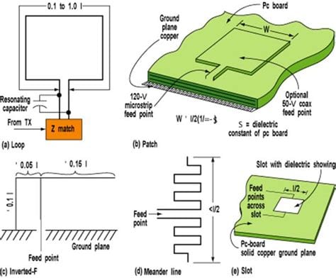
- Inverted-F Antenna (IFA): IFAs are compact, low-profile antennas that can be easily integrated into PCBs. They consist of a radiating element, a ground plane, and a shorting pin.
- Planar Inverted-F Antenna (PIFA): PIFAs are similar to IFAs but have a planar radiating element, making them even more compact. They are well-suited for dual band applications.
- Monopole Antenna: Monopole antennas are simple, omnidirectional antennas that can be designed for dual band operation by using techniques such as meandering or loading.
- Slot Antenna: Slot antennas are formed by cutting a slot in the ground plane of the PCB. They can be designed for dual band operation by adjusting the slot dimensions and adding parasitic elements.
Antenna Dimensions and Placement
The dimensions and placement of the antenna on the PCB are critical factors in achieving the desired performance. The following guidelines should be considered:
- Antenna size: The size of the antenna should be optimized for the target frequency bands. Lower frequencies require larger antennas, while higher frequencies can be accommodated by smaller antennas.
- Ground plane: The ground plane size and shape can significantly impact the antenna’s performance. A larger ground plane generally improves the antenna’s efficiency and bandwidth.
- Clearance: Sufficient clearance should be maintained between the antenna and other components on the PCB to minimize interference and coupling.
- Placement: The antenna should be placed away from noise sources, such as digital circuits and power supplies, to reduce EMI.
Substrate Selection and Stackup
The choice of substrate material and the PCB stackup can affect the antenna’s performance and EMI characteristics. Consider the following factors:
- Dielectric constant (εr): A higher dielectric constant allows for smaller antenna sizes but may reduce bandwidth and efficiency.
- Loss tangent (tanδ): A lower loss tangent is desirable to minimize dielectric losses and improve antenna efficiency.
- Substrate thickness: Thinner substrates can improve antenna bandwidth but may increase fabrication complexity and cost.
- Stackup: The number of layers and their arrangement in the PCB stackup can impact the antenna’s performance and EMI. Proper grounding and shielding techniques should be employed to minimize interference.

EMI Considerations in Dual Band PCB Antenna Design
Sources of EMI
EMI in dual band PCB antenna designs can arise from various sources, including:
- Digital circuits: High-speed digital circuits, such as microprocessors and memory, can generate significant EMI.
- Power supplies: Switching power supplies and voltage regulators can produce high-frequency noise that can interfere with the antenna.
- Other RF components: Nearby RF components, such as power amplifiers and filters, can couple energy into the antenna, causing interference.
EMI Reduction Techniques
To minimize EMI in dual band PCB antenna designs, several techniques can be employed:
- Grounding and shielding: Proper grounding and shielding techniques, such as using ground planes, via stitching, and shielding cans, can help contain EMI and prevent it from coupling into the antenna.
- Filtering: EMI filters, such as LC filters and ferrite beads, can be used to suppress high-frequency noise from power supplies and digital circuits.
- Decoupling: Adequate decoupling capacitors should be placed close to noise sources to minimize the propagation of high-frequency noise.
- Layout optimization: The PCB layout should be optimized to minimize the coupling between the antenna and potential EMI sources. This can be achieved by keeping sensitive traces away from noise sources and using orthogonal routing whenever possible.
Simulation and Measurement
To ensure that the dual band PCB antenna design meets the desired performance and EMI requirements, simulation and measurement techniques should be employed:
- Electromagnetic simulation: 3D electromagnetic simulation tools, such as Ansys HFSS or CST Studio Suite, can be used to model the antenna and predict its performance and EMI characteristics.
- Network analyzer measurements: A vector network analyzer (VNA) can be used to measure the antenna’s return loss, bandwidth, and isolation between the two frequency bands.
- EMI testing: EMI testing, such as conducted and radiated emissions tests, should be performed to ensure that the design complies with the relevant EMC standards (e.g., FCC, CE, CISPR).
Best Practices for Dual Band PCB Antenna Design
- Start with a well-established antenna topology and adapt it for dual band operation.
- Optimize the antenna dimensions and placement through parametric simulations.
- Choose a suitable substrate material and stackup based on the performance and EMI requirements.
- Employ proper grounding, shielding, and filtering techniques to minimize EMI.
- Optimize the PCB layout to reduce coupling between the antenna and potential EMI sources.
- Validate the design through electromagnetic simulations and measurements.
- Perform EMI testing to ensure compliance with the relevant EMC standards.
Conclusion
Designing a dual band PCB antenna that maintains low EMI levels requires careful consideration of antenna topology, dimensions, placement, substrate selection, and layout optimization. By following the guidelines and best practices outlined in this article, designers can create compact, cost-effective, and EMI-compliant dual band PCB antennas for a wide range of wireless applications.
Frequently Asked Questions (FAQ)
-
What are the main challenges in designing a dual band PCB antenna?
The main challenges in designing a dual band PCB antenna include achieving good performance at both frequency bands, maintaining a compact size, and minimizing EMI. -
How does the choice of substrate material affect the antenna’s performance?
The substrate material’s dielectric constant and loss tangent can impact the antenna’s size, bandwidth, and efficiency. A higher dielectric constant allows for smaller antennas but may reduce bandwidth and efficiency, while a lower loss tangent minimizes dielectric losses and improves efficiency. -
What are some common EMI reduction techniques for dual band PCB antennas?
Common EMI reduction techniques include proper grounding and shielding, filtering, decoupling, and layout optimization. These techniques help contain EMI and prevent it from coupling into the antenna. -
Why is it important to perform electromagnetic simulations and measurements?
Electromagnetic simulations and measurements are essential for predicting the antenna’s performance and EMI characteristics, optimizing the design, and ensuring compliance with the relevant EMC standards. -
Can a single dual band PCB antenna support more than two frequency bands?
While a dual band PCB antenna is designed to operate efficiently at two distinct frequency bands, it is possible to extend the concept to support more than two bands. However, this increases the design complexity and may require trade-offs in terms of performance and size.
No responses yet