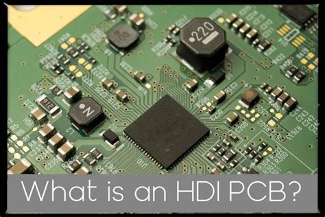
Basics of HDI PCB Cost Drivers
To understand how to reduce HDI PCB costs, it’s important to recognize the key factors that influence the price:
| Cost Factor | Description | Impact on Price |
|---|---|---|
| Layer Count | Higher layer counts increase complexity | More layers = higher cost |
| Via Structure | Buried, blind, and micro vias are more difficult than through-hole | Complex via structures increase cost |
| Line Width/Spacing | Ultra-fine lines and tight spacing require precision processes | Tighter tolerances raise costs |
| Material Selection | High-speed, high-frequency, or thermally demanding applications may require premium materials | Specialty materials are more expensive |
| Surface Finishes | Advanced finishes like ENIG are more involved than standard HASL | Sophisticated surface finishes add cost |
| Panel Utilization | Inefficient panelization leaves wasted board space | Poor utilization increases cost per PCB |
By making smart decisions in each of these areas, it’s possible to significantly decrease the price of HDI PCBs without cutting corners on quality. The following sections will explain cost-reduction strategies in more detail.
Optimize Your Layer Stack-Up
One of the most effective ways to lower HDI PCB cost is to minimize the number of layers in your stack-up. Each additional layer increases manufacturing complexity, material usage, and processing time. To reduce layer count without sacrificing functionality:
- Place all power and ground planes on the inner layers
- Route signals on outer layers whenever possible
- Use blind and buried vias judiciously to make connections between inner layers
- Consider using passive components embedded in the PCB substrate
For example, moving from a 10-layer to an 8-layer HDI design can cut costs by 20-30% in many cases. However, be careful not to over-constrain the layout, as this can make routing more difficult and introduce signal integrity issues. Work closely with your manufacturer to determine the optimal layer stack-up for your specific application.

Simplify Your Via Structure
The vias in an HDI PCB are a major determinant of cost, as they require specialized equipment and processes to fabricate. Through-hole vias that span the entire board thickness are the simplest and cheapest, followed by blind vias that connect outer to inner layers, then buried vias between inner layers only. Microvias less than 6 mils in diameter drilled with lasers are the most expensive.
To minimize via costs in your HDI PCB:
- Avoid buried vias unless absolutely necessary for your design
- Use blind vias to access inner layers rather than through-holes
- Combine blind and through-hole vias to span multiple layers
- Enlarge your microvias as much as possible to at least 8 mil diameter
- Reduce the aspect ratio of vias to less than 6:1 for easier manufacturing
The table below shows an example of how via type impacts cost for a 10-layer HDI board:
| Via Type | Relative Cost |
|---|---|
| Through Hole Only | 1.0 |
| Blind Vias | 1.2 |
| Buried Vias | 1.5 |
| Microvias | 2.0 |
By optimizing your via structure, you can shave 10-15% off the cost of the PCB without any reduction in performance. Be sure to follow your manufacturer’s design rules for via size, spacing, and aspect ratio to ensure high yields and reliability.

Use Thicker Copper Weight
The thickness of the copper foil used in an HDI PCB, known as its weight, also factors heavily into the cost equation. Thinner copper, such as ½ oz or 9 μm, enables finer line widths and tighter spacing but also requires more precise processing and control to achieve high yields. This drives up costs and can impact signal integrity if not executed properly.
Where possible, consider using 1 oz (18 μm) or thicker copper instead to reduce manufacturing costs. The advantages of heavy copper include:
- Less expensive base materials
- Wider minimum line width and spacing
- Improved current carrying capacity and lower resistance
- Better heat dissipation for high-power components
- More mechanically robust for assembly and rework
Using 1 oz copper can reduce HDI PCB costs by 5-10% compared to ½ oz. For non-critical traces, you may even be able to use 2 oz copper, although this will constrain routing density. Consult with your fabricator on the capabilities and tradeoffs of different copper weights.

Select Cost-Effective Materials
The laminate and prepreg materials used in an HDI PCB Stack-Up play a significant role in determining its electrical, thermal, and mechanical properties. However, specialty materials designed for high-speed digital, RF/microwave, or thermally demanding applications can also add substantial cost to the board.
For more budget-friendly options, consider using:
- Standard FR-4 laminates instead of high-speed materials
- Halogen-free FR-4 rather than ceramics for low-loss
- Mid-Tg or high-Tg FR-4 instead of polyimides for thermal resistance
- No-flow or low-flow prepregs rather than laser-drillable for HDI
Work with your fabricator to identify material substitutions that can reduce cost while still meeting your performance needs. The table below shows some common high-end materials and lower-cost alternatives:
| High-End Material | Benefits | Lower-Cost Alternative |
|---|---|---|
| Isola I-Speed | Ultra-low loss for 56G+ speeds | Mid-Tg FR-4 |
| Rogers 4350B | Stable Dk for mmWave frequencies | Taconic FastRise |
| Polyimide | Tg of 250°C for harsh environments | High-Tg FR-4 |
| PTFE | Excellent thermal resistance | Hydrocarbon ceramic |
Opting for standard or alternative materials can trim 10-20% off your HDI PCB material costs. Just be sure to carefully evaluate any substitutions to ensure they can handle your application requirements over the full product lifecycle.
Streamline Your Testing Strategy
Rigorous testing is essential for assuring the quality and reliability of HDI PCBs. However, over-specifying your test requirements can significantly increase costs without adding much value. To optimize your HDI testing:
- Only perform electrical tests that are critical for your application
- Use go/no-go DC testing instead of full parametric testing where possible
- Minimize the use of custom test coupons or non-standard hole sizes
- Limit destructive cross-sectioning to a sample of boards rather than 100%
- Consider in-circuit testing to find assembly defects vs. board-level functional testing
Also, be sure to design for testability from the start by including test points, probe targets, and access to all nets. This will help streamline testing and reduce the time and cost needed for validation.
Panelize for Maximum Efficiency
Panelization refers to the grouping of multiple PCBs onto a larger panel for fabrication. Effective panelization maximizes the number of boards that can fit in a panel, thereby decreasing the cost per PCB. However, it’s not always obvious how to arrange the boards for optimal panel utilization.
Follow these best practices to get the most out of your panels:
- Choose a panel size that matches your manufacturer’s equipment, typically 18″ x 24″
- Minimize the spacing between boards while still allowing for proper tooling and handling
- Rotate boards in different directions to fit more in odd-shaped panels
- Place any test coupons or tooling holes in the panel borders rather than between boards
- Consider panelizing multiple different designs in the same panel to share NRE Costs
Optimizing your panelization can increase board density by 15-20%, directly reducing the cost per PCB by an equivalent amount. Work with your fabricator to identify the most efficient panelization scheme for your particular HDI design.
Partner with the Right Manufacturer
Ultimately, controlling HDI PCB costs requires close collaboration between the designer and fabricator. The right manufacturing partner will have the experience and expertise to guide you through the cost-reduction process while still delivering high-quality boards. When selecting an HDI PCB supplier, look for:
- A proven track record of successful HDI projects
- Robust DFM capabilities to identify cost-saving opportunities
- State-of-the-art equipment for fine line and space, microvias, etc.
- Skilled engineers who can offer design and material selection advice
- Flexible service options for prototypes through volume production
A true manufacturing partner will work with you to optimize your HDI design for cost, manufacturability, and reliability. Don’t be afraid to ask for guidance and suggestions throughout the development process.
FAQs
Q: How much can I expect to save by optimizing my HDI PCB Design for cost?
A: The total cost savings will depend on the specifics of your design, but reductions of 20-40% are possible by implementing the strategies outlined in this article. The biggest opportunities are typically in reducing layer count, simplifying via structure, and optimizing panelization.
Q: Will reducing the cost of my HDI PCB impact its reliability or performance?
A: Not if done properly. The key is to work closely with your manufacturer to identify areas where costs can be safely reduced without compromising quality. Many cost-saving measures, such as using thicker copper or standard materials, can actually improve reliability.
Q: How do I know if my HDI PCB design is a good candidate for cost reduction?
A: Any HDI design can benefit from a cost-optimization review. However, the most promising candidates are typically those with high layer counts, complex via structures, tight line and space, or expensive materials. Designs with poor panel utilization or excessive testing requirements are also good targets.
Q: What if I need to use specialty materials or processes for my HDI application?
A: In some cases, the performance requirements of an application may necessitate the use of high-end materials or processes that add cost. The goal should be to minimize the use of these specialty items to only what is truly needed. Work with your manufacturer to identify potential lower-cost alternatives that can still meet your needs.
Q: How long does it take to optimize an HDI PCB design for cost?
A: The time required will vary depending on the complexity of the design and the extent of the changes needed. However, most cost-optimization efforts can be completed in a matter of weeks, especially if done early in the design process. The key is to involve your manufacturer as early as possible to identify and implement cost-saving opportunities.
Conclusion
HDI PCBs are a powerful enabling technology for today’s advanced electronics, but their complexity and precision can also drive up costs. By taking a strategic approach to design and manufacturing, it’s possible to significantly reduce the cost of HDI PCBs without sacrificing quality or reliability.
Key strategies for HDI cost reduction include:
- Optimizing layer stack-up and via structure
- Using thicker copper weights and standard materials
- Streamlining testing and panelization
- Partnering with an experienced HDI manufacturer
By working closely with your fabricator and implementing these techniques, you can minimize the cost of your HDI PCBs while still delivering the performance and reliability your application demands. Don’t let the fear of high costs hold you back from leveraging the full potential of HDI technology.
No responses yet