What is Tented-via Clearance and Why is it Important?
Tented-via clearance, also known as solder mask web or solder mask bridge, refers to the distance between the edge of a via hole and the edge of the surrounding solder mask opening on a printed circuit board (PCB). This clearance plays a crucial role in ensuring the reliability and manufacturability of PCBs, especially when using tented vias.
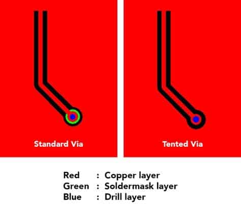
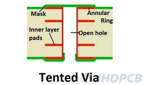
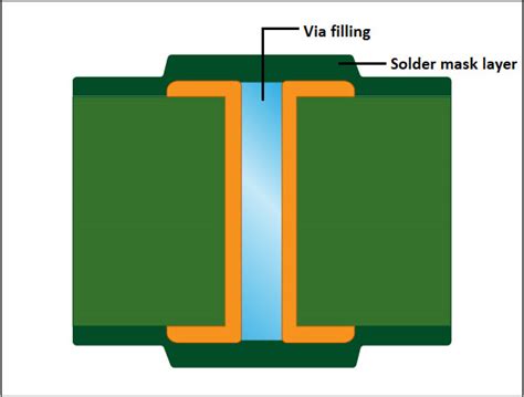
Tented vias are vias that are completely covered by solder mask on both sides of the PCB. This technique is used to protect the vias from environmental factors, prevent solder from wicking into the via during the soldering process, and improve the overall aesthetic appearance of the PCB.
Proper tented-via clearance is essential for several reasons:
-
Solder mask adhesion: Adequate clearance allows for better adhesion of the solder mask to the PCB surface around the via, reducing the risk of solder mask delamination or peeling.
-
Manufacturability: Sufficient clearance ensures that the solder mask can be applied consistently and accurately during the PCB fabrication process, minimizing the occurrence of defects such as solder mask bridges or solder mask openings that are too small.
-
Electrical integrity: Appropriate tented-via clearance helps maintain the electrical integrity of the PCB by preventing short circuits or Signal Integrity issues caused by insufficient solder mask coverage.
-
Reliability: Proper clearance contributes to the overall reliability of the PCB by minimizing stress on the solder mask around the vias during thermal cycling and mechanical stresses.
Factors Affecting Tented-via Clearance
Several factors influence the choice of tented-via clearance in PCB Design:
-
PCB fabrication capabilities: The minimum achievable tented-via clearance depends on the capabilities of the PCB manufacturer. Advanced manufacturing processes can achieve smaller clearances, while basic processes may require larger clearances.
-
Via size: The size of the via hole affects the required clearance. Smaller vias generally require smaller clearances, while larger vias may need larger clearances to ensure proper solder mask coverage.
-
Solder mask type: The type of solder mask used (liquid photoimageable, dry film, or ink-jet) can impact the minimum achievable clearance. Liquid photoimageable solder masks typically allow for smaller clearances compared to other types.
-
PCB thickness: The thickness of the PCB can influence the tented-via clearance. Thicker PCBs may require larger clearances to accommodate the increased depth of the via hole.
-
PCB application: The intended application of the PCB may dictate the required tented-via clearance. For example, high-reliability applications or PCBs subjected to harsh environments may require larger clearances to ensure long-term performance.

Recommended Tented-via Clearance Values
The recommended tented-via clearance values vary depending on the PCB manufacturer and the specific design requirements. However, the following table provides general guidelines for minimum tented-via clearances based on via hole size:
| Via Hole Size (mm) | Minimum Tented-via Clearance (mm) |
|---|---|
| 0.2 – 0.4 | 0.05 – 0.075 |
| 0.4 – 0.6 | 0.075 – 0.1 |
| 0.6 – 0.8 | 0.1 – 0.125 |
| 0.8 – 1.0 | 0.125 – 0.15 |
| 1.0 – 1.2 | 0.15 – 0.175 |
It is important to consult with your PCB manufacturer to determine their specific capabilities and recommendations for tented-via clearances.

Designing for Optimal Tented-via Clearance
To ensure optimal tented-via clearance in your PCB design, consider the following best practices:
-
Collaborate with your PCB manufacturer: Engage with your PCB manufacturer early in the design process to understand their capabilities and recommendations for tented-via clearances. This collaboration can help you make informed decisions and avoid potential manufacturability issues.
-
Use appropriate via sizes: Select via sizes that are compatible with your PCB manufacturer’s capabilities and the requirements of your design. Avoid using excessively small or large vias that may complicate the tenting process.
-
Consider solder mask type: Choose a solder mask type that is suitable for your design requirements and allows for the desired tented-via clearance. Liquid photoimageable solder masks are often preferred for their ability to achieve smaller clearances.
-
Maintain consistent clearances: Ensure that the tented-via clearances are consistent throughout your PCB design. Inconsistent clearances can lead to manufacturability issues and potential reliability problems.
-
Perform design rule checks (DRC): Utilize DRC tools in your PCB design software to verify that your tented-via clearances meet the specified design rules. This step helps identify and correct any clearance violations before sending the design for manufacturing.
-
Consider alternative via protection methods: In some cases, tented vias may not be the most suitable option for your design. Consider alternative via protection methods, such as via filling or via capping, which can provide similar benefits without the need for tented-via clearances.

Tented-via Clearance and High-speed PCB Design
In high-speed PCB designs, tented vias can play a crucial role in maintaining signal integrity and minimizing signal distortion. However, the tented-via clearance must be carefully considered to ensure optimal performance.
-
Impedance control: Tented vias can affect the impedance of high-speed signals passing through the via. Insufficient tented-via clearance can lead to impedance discontinuities, causing signal reflections and degrading signal quality. Ensure that the tented-via clearance is accounted for in your impedance calculations and simulations.
-
Stubs and resonance: Tented vias can create stubs, which are unused portions of the via that can cause resonance and signal degradation at high frequencies. To minimize the impact of stubs, consider using techniques such as back-drilling or blind/buried vias in conjunction with tented vias.
-
Signal coupling: Tented vias can also contribute to signal coupling between adjacent vias, especially if the clearances are too small. Ensure that the tented-via clearance is sufficient to minimize coupling and Crosstalk between high-speed signals.
-
Simulation and analysis: Perform rigorous signal integrity simulations and analysis to evaluate the impact of tented-via clearances on your high-speed design. Use tools such as 3D electromagnetic simulation software to accurately model the tented vias and assess their performance.
FAQ
-
What is the minimum recommended tented-via clearance?
The minimum recommended tented-via clearance depends on various factors such as via size, PCB thickness, and manufacturing capabilities. Generally, the minimum clearance ranges from 0.05 mm to 0.175 mm, depending on the via hole size. However, it is essential to consult with your PCB manufacturer for their specific recommendations. -
Can tented vias be used in high-voltage applications?
Yes, tented vias can be used in high-voltage applications, but special considerations must be made. The tented-via clearance should be increased to provide adequate insulation and prevent voltage breakdown. Additionally, the solder mask material should be selected based on its dielectric strength and ability to withstand the required voltage levels. -
How does the choice of solder mask affect tented-via clearance?
The choice of solder mask can impact the achievable tented-via clearance. Liquid photoimageable solder masks generally allow for smaller clearances compared to dry film or ink-jet solder masks. This is due to the higher resolution and better control over the solder mask openings that can be achieved with liquid photoimageable masks. -
Can tented vias be used on both sides of the PCB?
Yes, tented vias can be used on both sides of the PCB. This is known as double-sided tenting. Double-sided tenting provides additional protection for the vias and can enhance the overall reliability of the PCB. However, it is important to ensure that the tented-via clearances are consistent on both sides of the board to avoid any manufacturing issues. -
What are the alternatives to tented vias for via protection?
There are several alternatives to tented vias for via protection, including: -
Via filling: The vias are filled with a conductive or non-conductive material to seal them and provide protection.
- Via capping: A small cap of copper or other material is placed over the via to protect it from the environment.
- Plugged vias: The vias are plugged with a non-conductive material, such as epoxy, to seal them and prevent solder wicking.
Each alternative has its own advantages and disadvantages, and the choice depends on the specific design requirements and manufacturing capabilities.
Conclusion
Tented-via clearance is a critical aspect of PCB design that ensures the reliability, manufacturability, and performance of tented vias. By understanding the factors affecting tented-via clearance, selecting appropriate clearance values, and following best practices for PCB design, engineers can create robust and high-quality PCBs that meet the demands of modern electronics.
When designing PCBs with tented vias, it is essential to collaborate with your PCB manufacturer, consider the specific requirements of your application, and perform thorough simulations and analyses to validate your design choices. By paying attention to tented-via clearance and other critical design aspects, you can enhance the overall quality and reliability of your PCB while minimizing the risk of manufacturing defects and performance issues.

No responses yet