Introduction to Signal Integrity
Signal integrity (SI) is a critical aspect of high-speed electronic design that ensures the quality and reliability of electrical signals as they propagate through interconnects, such as printed circuit board (PCB) traces, cables, and connectors. In today’s digital systems, where data rates continue to increase and signal rise times decrease, maintaining signal integrity becomes increasingly challenging. Poor signal integrity can lead to data corruption, system malfunctions, and reduced overall performance.
What is Signal Integrity?
Signal integrity refers to the ability of an electrical signal to maintain its intended characteristics as it travels from the source to the receiver. These characteristics include:
– Signal shape and timing
– Voltage levels
– Rise and fall times
– Frequency content
When signal integrity is compromised, the received signal may differ significantly from the transmitted signal, leading to errors in data interpretation and system failures.
Importance of Signal Integrity in High-Speed Designs
As digital systems continue to push the boundaries of speed and performance, signal integrity becomes increasingly critical. Some key reasons why signal integrity is crucial in high-speed designs include:
-
Higher data rates: With the demand for faster data transmission, signal frequencies and data rates continue to increase. Higher frequencies are more susceptible to signal integrity issues, such as attenuation, distortion, and crosstalk.
-
Smaller feature sizes: As IC technology advances, transistor sizes and interconnect dimensions continue to shrink. Smaller geometries are more sensitive to signal integrity problems, such as increased resistance, capacitance, and inductance.
-
Increased complexity: Modern electronic systems are becoming more complex, with higher component densities and more intricate PCB layouts. This complexity can exacerbate signal integrity issues, as signals must navigate through more complex interconnect structures.
-
Tighter timing margins: Higher data rates and smaller feature sizes result in tighter timing margins for signal propagation. Even small signal integrity issues can cause timing violations and lead to system failures.
Common Signal Integrity Problems
Several signal integrity issues can arise in high-speed designs, each with its own set of causes and effects. Some of the most common signal integrity problems include:
Reflections and Impedance Mismatch
Reflections occur when a signal encounters an impedance mismatch along its propagation path. When the characteristic impedance of the transmission line does not match the source or load impedance, a portion of the signal energy is reflected back towards the source. These reflections can cause signal distortion, ringing, and overshoot, leading to data corruption and timing issues.
Causes of Reflections and Impedance Mismatch
- Improper termination: When the load impedance does not match the characteristic impedance of the transmission line, reflections occur at the load.
- Discontinuities in the signal path: Abrupt changes in the geometry of the interconnect, such as vias, connectors, or stubs, can cause impedance mismatches and reflections.
- Inadequate PCB layout: Poor PCB layout techniques, such as improper trace widths, spacing, or routing, can lead to impedance mismatches.
Mitigating Reflections and Impedance Mismatch
- Proper termination: Use appropriate termination techniques, such as series, parallel, or differential termination, to match the load impedance to the characteristic impedance of the transmission line.
- Impedance matching: Ensure that the characteristic impedance of the interconnect remains consistent throughout the signal path. This can be achieved through proper PCB stackup design and controlled impedance routing.
- Minimize discontinuities: Avoid abrupt changes in the signal path geometry, such as unnecessary vias or stubs. Use smooth transitions and maintain consistent trace widths and spacing.
Crosstalk
Crosstalk is the unintended coupling of energy between adjacent signal traces. When a signal on one trace induces voltage or current on a nearby trace, it can lead to signal distortion, noise, and timing issues. Crosstalk becomes more pronounced at higher frequencies and with smaller trace spacing.
Types of Crosstalk
- Near-end crosstalk (NEXT): Crosstalk that occurs at the same end of the transmission line as the source of the interference.
- Far-end crosstalk (FEXT): Crosstalk that appears at the opposite end of the transmission line from the source of the interference.
Causes of Crosstalk
- Electromagnetic coupling: The electric and magnetic fields generated by a signal on one trace can couple to adjacent traces, inducing unwanted voltage or current.
- Inadequate trace spacing: Smaller trace spacing increases the likelihood of crosstalk, as the coupling between traces becomes stronger.
- Poor layer stacking: Improper arrangement of signal and reference layers in the PCB stackup can increase crosstalk.
Mitigating Crosstalk
- Increase trace spacing: Maintain adequate spacing between signal traces to minimize electromagnetic coupling. Use simulation tools to determine the optimal trace spacing for your design.
- Optimize layer stacking: Arrange signal and reference layers in the PCB stackup to minimize crosstalk. Use ground planes to shield signal layers and provide return paths for high-frequency currents.
- Use guard traces: Place grounded guard traces between sensitive signal traces to reduce crosstalk.
- Employ differential signaling: Use differential signaling techniques, such as LVDS or CML, to minimize the impact of crosstalk on signal integrity.
Attenuation and Loss
Attenuation is the reduction in signal strength as it propagates through the interconnect. High-frequency signals are particularly susceptible to attenuation due to the frequency-dependent losses in the transmission line. Attenuation can lead to reduced signal-to-noise ratio (SNR), increased jitter, and data corruption.
Types of Loss
- Conductor loss: Caused by the resistance of the conductors in the interconnect. Increases with frequency due to the skin effect.
- Dielectric loss: Caused by the dissipation of energy in the dielectric material surrounding the conductors. Increases with frequency.
Causes of Attenuation and Loss
- Frequency-dependent losses: As signal frequencies increase, conductor and dielectric losses become more significant.
- Long trace lengths: Longer traces result in greater attenuation, as the signal has to travel a greater distance through the lossy medium.
- Inadequate PCB materials: PCB materials with high dielectric loss tangents or poor high-frequency performance can exacerbate attenuation.
Mitigating Attenuation and Loss
- Use low-loss PCB materials: Select PCB materials with low dielectric loss tangents and good high-frequency performance, such as low-loss laminates or PTFE-based materials.
- Minimize trace lengths: Keep signal traces as short as possible to reduce the overall attenuation.
- Employ equalization techniques: Use equalization circuits, such as pre-emphasis or de-emphasis, to compensate for high-frequency losses and improve signal quality.
- Consider repeaters or redrivers: For long trace lengths, use repeaters or redrivers to regenerate the signal and maintain signal integrity.
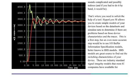
Signal Integrity Analysis and Simulation
To ensure signal integrity in high-speed designs, it is essential to perform thorough analysis and simulation during the design phase. Signal integrity analysis helps identify potential issues early in the design process, allowing for timely mitigation and optimization.
Pre-Layout Analysis
Pre-layout analysis involves evaluating the signal integrity of a design before the physical layout is created. This analysis helps establish design constraints and guidelines for the PCB layout.
Schematic Review
- Check for proper termination: Ensure that all transmission lines are properly terminated to minimize reflections and impedance mismatches.
- Verify power and ground distribution: Ensure that power and ground nets are adequately sized and distributed to minimize voltage drops and maintain signal integrity.
Topology Analysis
- Evaluate signal routing: Analyze the proposed signal routing to identify potential issues, such as excessive via count, stubs, or improper trace geometry.
- Assess crosstalk risk: Identify areas where crosstalk may be a concern, such as high-density routing or long parallel trace runs.
Post-Layout Analysis
Post-layout analysis involves simulating the signal integrity of the design after the physical layout has been created. This analysis helps validate the design and identify any remaining signal integrity issues.
Impedance Analysis
- Verify controlled impedance: Ensure that the PCB traces maintain the desired characteristic impedance throughout the signal path.
- Check for discontinuities: Identify any impedance discontinuities caused by vias, connectors, or changes in trace geometry.
Crosstalk Analysis
- Simulate crosstalk: Use 3D field solvers or SPICE-based simulators to analyze crosstalk between adjacent traces.
- Evaluate the impact of crosstalk: Determine the effect of crosstalk on signal quality and timing, and assess whether additional mitigation measures are necessary.
Loss Analysis
- Simulate frequency-dependent losses: Use simulation tools to model the frequency-dependent losses in the interconnect, including conductor and dielectric losses.
- Evaluate the impact of losses: Assess the effect of losses on signal quality, jitter, and timing, and determine if equalization or other mitigation techniques are required.
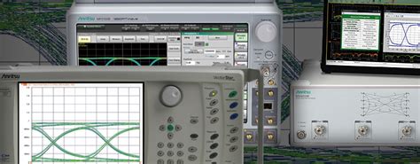
Simulation Tools and Techniques
Several simulation tools and techniques are available for signal integrity analysis, each with its own strengths and applications.
SPICE-Based Simulators
- Examples: HSPICE, LTspice, PSpice
- Application: Time-domain analysis of lumped and distributed element circuits, including transmission lines, terminations, and passive components.
3D Field Solvers
- Examples: Ansys HFSS, Cadence Sigrity, Mentor Graphics HyperLynx
- Application: Full-wave electromagnetic simulation of complex interconnect structures, including vias, connectors, and nonuniform trace geometries.
Statistical Analysis
- Examples: Mentor Graphics HyperLynx DRC, Cadence Sigrity
- Application: Perform statistical analysis of signal integrity, considering manufacturing variations and tolerances, to ensure robust design performance.

Best Practices for Signal Integrity
To maintain signal integrity in high-speed designs, designers should follow a set of best practices throughout the design process. These practices help minimize signal integrity issues and ensure reliable system performance.
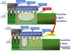
PCB Layout Guidelines
- Route signals over continuous reference planes: Provide uninterrupted return paths for high-frequency currents by routing signals over solid ground or power planes.
- Minimize trace lengths: Keep signal traces as short as possible to reduce attenuation and signal propagation delay.
- Match trace lengths: For critical signals, such as clock or differential pairs, match the trace lengths to maintain signal synchronization and minimize skew.
- Avoid sharp corners: Use 45-degree angles or smooth curves for trace routing to minimize reflections and impedance discontinuities.
- Provide adequate via spacing: Maintain sufficient spacing between vias to minimize crosstalk and signal distortion.
Stackup Design
- Use dedicated signal layers: Assign critical signals to dedicated layers, separated by ground or power planes, to minimize crosstalk and provide shielding.
- Minimize dielectric thickness: Use thin dielectric layers between signal and reference planes to reduce inductance and improve signal integrity.
- Consider asymmetric stackups: For designs with a mix of high-speed and low-speed signals, consider using asymmetric stackups to optimize the performance of each signal type.
Termination Strategies
- Use appropriate termination: Select the appropriate termination strategy, such as series, parallel, or differential termination, based on the signal characteristics and impedance requirements.
- Place terminations close to the receiver: Locate termination resistors as close to the receiver as possible to minimize reflections and signal distortion.
- Consider on-die termination: For high-speed designs, consider using on-die termination (ODT) to reduce the impact of package and board-level parasitics.
Power Distribution Network (PDN) Design
- Provide adequate decoupling: Use decoupling capacitors to provide a low-impedance path for high-frequency currents and minimize power supply noise.
- Optimize capacitor placement: Place decoupling capacitors close to the power pins of ICs to minimize the loop inductance and improve high-frequency performance.
- Use power and ground planes: Use solid power and ground planes to provide low-impedance power distribution and minimize voltage drops.
Signal Conditioning and Equalization
- Consider pre-emphasis: Use pre-emphasis techniques, such as driver pre-emphasis or FIR filtering, to boost high-frequency components of the signal and compensate for losses.
- Employ de-emphasis: Use de-emphasis techniques, such as receiver equalization or CTLE, to attenuate low-frequency components and improve signal quality.
- Implement adaptive equalization: For high-speed serial links, consider using adaptive equalization techniques, such as DFE or FFE, to dynamically adjust the equalization based on the channel characteristics.
FAQ
- What is the difference between near-end crosstalk (NEXT) and far-end crosstalk (FEXT)?
-
Near-end crosstalk (NEXT) occurs when the coupling between adjacent traces is measured at the same end of the transmission line as the source of the interference. Far-end crosstalk (FEXT) occurs when the coupling is measured at the opposite end of the transmission line from the source of the interference.
-
How does the skin effect impact signal integrity at high frequencies?
-
The skin effect is a phenomenon where high-frequency currents tend to flow on the outer surface of a conductor, rather than uniformly throughout its cross-section. As a result, the effective resistance of the conductor increases with frequency, leading to higher attenuation and signal distortion. To mitigate the impact of the skin effect, designers can use wider traces, lower-loss PCB materials, or consider using differential signaling techniques.
-
What is the purpose of a ground plane in a PCB stackup?
-
A ground plane serves multiple purposes in a PCB stackup. It provides a low-impedance return path for high-frequency currents, minimizing loop inductance and reducing electromagnetic interference (EMI). Additionally, a ground plane acts as a shield between signal layers, reducing crosstalk and improving signal isolation. By maintaining a consistent reference plane, a ground plane also helps control the characteristic impedance of the transmission lines.
-
What is the difference between pre-emphasis and de-emphasis in signal conditioning?
-
Pre-emphasis is a signal conditioning technique where the high-frequency components of the signal are boosted before transmission to compensate for the anticipated high-frequency losses in the channel. De-emphasis, on the other hand, is a technique where the low-frequency components of the signal are attenuated at the receiver to equalize the frequency response and improve signal quality. Pre-emphasis is typically applied at the transmitter, while de-emphasis is applied at the receiver.
-
How can simulation tools help in ensuring signal integrity in high-speed designs?
- Simulation tools play a crucial role in ensuring signal integrity in high-speed designs by allowing designers to analyze and optimize the performance of the system before physical implementation. SPICE-based simulators enable time-domain analysis of circuits, including transmission lines, terminations, and passive components. 3D field solvers, such as Ansys HFSS or Cadence Sigrity, provide full-wave electromagnetic simulation of complex interconnect structures, helping designers identify and mitigate issues related to reflections, crosstalk, and losses. Statistical analysis tools, like Mentor Graphics HyperLynx DRC or Cadence Sigrity, allow designers to perform statistical simulations considering manufacturing variations and tolerances, ensuring a robust design that meets signal integrity requirements.
Conclusion
Signal integrity is a critical aspect of high-speed electronic design that ensures the quality and reliability of electrical signals as they propagate through interconnects. As data rates continue to increase and signal rise times decrease, maintaining signal integrity becomes increasingly challenging. Common signal integrity problems, such as reflections, crosstalk, and attenuation, can lead to data corruption, system malfunctions, and reduced overall performance.
To address these challenges, designers must employ a combination of analysis, simulation, and best practices throughout the design process. Pre-layout and post-layout analyses help identify potential signal integrity issues early in the design phase, allowing for timely mitigation and optimization. Simulation tools, such as SPICE-based simulators, 3D field solvers, and statistical analysis tools, enable designers to evaluate the performance of the system and ensure that signal integrity requirements are met.
Best practices for maintaining signal integrity include following proper PCB layout guidelines, optimizing stackup design, selecting appropriate termination strategies, implementing robust power distribution networks, and employing signal conditioning and equalization techniques. By adhering to these best practices and leveraging the available tools and techniques, designers can successfully overcome the signal integrity challenges associated with high-speed designs and deliver reliable, high-performance electronic systems.
No responses yet