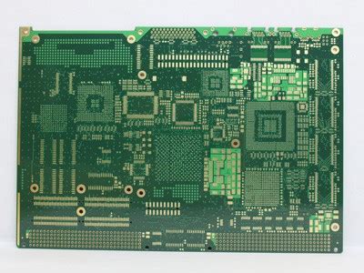
What are HDI PCBs?
HDI PCBs are characterized by their high density of interconnects, which allows for the integration of more components and functionality into a smaller space. The main features of HDI PCBs include:
- Fine pitch traces and spaces (typically less than 100 microns)
- Microvias (blind, buried, or stacked) for interconnection between layers
- Thin dielectric materials for reduced layer thickness
- Copper-filled microvias for improved thermal and electrical performance
These features enable HDI PCBs to achieve higher routing density, improved signal integrity, and better heat dissipation compared to traditional PCBs.
Advantages of HDI PCBs
HDI PCBs offer several advantages over conventional PCB designs:
-
Miniaturization: The high density of interconnects allows for smaller PCB sizes, which is crucial for modern electronic devices that demand compact form factors.
-
Enhanced performance: The use of fine pitch traces and microvias reduces signal path lengths, resulting in improved signal integrity and reduced electromagnetic interference (EMI).
-
Increased functionality: With the ability to integrate more components and features into a smaller space, HDI PCBs enable the creation of more complex and multi-functional electronic devices.
-
Improved reliability: The use of copper-filled microvias and advanced materials enhances the thermal and mechanical stability of HDI PCBs, leading to higher reliability and longer product life.
-
Cost-effectiveness: Although the initial manufacturing costs may be higher, HDI PCBs can ultimately lead to cost savings by reducing the overall PCB size, simplifying assembly processes, and improving yields.

HDI PCB Manufacturing Process
The manufacturing process for HDI PCBs involves several advanced techniques and technologies:
1. Substrate Preparation
The process begins with the selection and preparation of the base substrate material, which is typically a thin, high-performance dielectric such as FR-4, polyimide, or liquid crystal polymer (LCP). The substrate is cleaned and inspected for defects before proceeding to the next step.
2. Copper Deposition
A thin layer of copper is deposited onto the substrate using electroless or electrolytic plating methods. This layer serves as the seed layer for subsequent copper plating steps.
3. Patterning and Etching
The desired circuit pattern is transferred onto the copper layer using photolithography techniques. A photoresist is applied, exposed through a photomask, and developed to create the desired pattern. The exposed copper is then etched away using chemical or plasma etching methods, leaving behind the desired traces and pads.
4. Microvia Formation
Microvias are formed using laser drilling, photovia, or plasma etching techniques. These microvias connect the different layers of the PCB and enable high-density interconnects.
5. Lamination and Pressing
Multiple patterned layers are aligned and laminated together using heat and pressure to form a multi-layer PCB stack. The lamination process ensures good adhesion between layers and prevents delamination issues.
6. Drilling and Plating
Through-holes are drilled in the laminated PCB stack to accommodate components and provide interconnection between layers. The holes are then plated with copper to create conductive paths.
7. Surface Finish
A surface finish, such as Electroless Nickel Immersion Gold (ENIG), Immersion Silver, or Organic Solderability Preservative (OSP), is applied to the exposed copper surfaces to prevent oxidation and improve solderability.
8. Solder Mask and Silkscreen
A solder mask is applied to protect the copper traces and prevent solder bridging during assembly. A silkscreen layer is then added to provide component placement markings and other visual information.
9. Electrical Testing
The completed HDI PCB undergoes rigorous electrical testing to ensure proper functionality and compliance with design specifications. This includes continuity tests, insulation resistance tests, and high-potential (HiPot) tests.

Applications of HDI PCBs
HDI PCBs find applications in a wide range of industries and products, including:
-
Consumer Electronics: Smartphones, tablets, wearables, and other portable devices heavily rely on HDI PCBs to achieve compact sizes and high performance.
-
Automotive Electronics: Advanced driver assistance systems (ADAS), infotainment systems, and other automotive electronics use HDI PCBs for reliable and space-efficient designs.
-
Medical Devices: Implantable devices, diagnostic equipment, and other medical electronics benefit from the miniaturization and reliability offered by HDI PCBs.
-
Aerospace and Defense: Avionics, satellite systems, and military electronics employ HDI PCBs for their high-performance and robust design requirements.
-
Industrial Automation: Factory automation systems, process control equipment, and other industrial electronics use HDI PCBs for compact and reliable designs.

Future Trends in HDI PCBs
As electronic devices continue to evolve and demand higher performance in smaller packages, HDI PCBs are expected to play an increasingly important role. Some of the future trends in HDI PCB technology include:
-
Advanced Materials: The development of new, high-performance dielectric materials and conductive inks will enable even finer feature sizes and improved electrical properties.
-
Embedded Components: The integration of passive components (resistors, capacitors, inductors) directly into the PCB substrate will further enhance miniaturization and performance.
-
3D Packaging: The use of 3D packaging techniques, such as package-on-package (PoP) and system-in-package (SiP), will allow for even higher levels of integration and functionality.
-
Flexible and Stretchable HDI PCBs: The development of flexible and stretchable HDI PCBs will enable new applications in wearable electronics, medical devices, and robotics.
-
Additive Manufacturing: The use of additive manufacturing techniques, such as 3D printing, will enable rapid prototyping and customization of HDI PCBs.
Frequently Asked Questions (FAQ)
1. What is the minimum feature size achievable with HDI PCBs?
HDI PCBs can achieve trace widths and spaces as small as 25-50 microns, depending on the specific manufacturing process and technology used.
2. How do HDI PCBs compare to traditional PCBs in terms of cost?
While HDI PCBs may have higher initial manufacturing costs due to the advanced processes and materials involved, they can ultimately lead to cost savings by reducing the overall PCB size, simplifying assembly, and improving yields.
3. What are the main challenges in designing HDI PCBs?
Some of the main challenges in designing HDI PCBs include managing signal integrity, ensuring proper thermal management, and adhering to strict manufacturing tolerances. Designers must also be familiar with the specific design rules and constraints associated with HDI PCB fabrication.
4. Can HDI PCBs be reworked or repaired?
Reworking or repairing HDI PCBs can be more challenging than traditional PCBs due to the fine features and dense interconnects. However, with proper techniques and equipment, such as precision soldering and microscopic inspection, HDI PCBs can be successfully reworked or repaired.
5. What are the environmental considerations for HDI PCBs?
HDI PCBs must comply with various environmental regulations, such as the Restriction of Hazardous Substances (RoHS) directive and the Registration, Evaluation, Authorization, and Restriction of Chemicals (REACH) regulation. Manufacturers must ensure that the materials and processes used in HDI PCB production are environmentally friendly and comply with these regulations.
Conclusion
High-Density Interconnect (HDI) printed circuit boards represent a significant advancement in PCB technology, enabling the creation of smaller, faster, and more complex electronic devices. With their fine pitch traces, microvias, and advanced materials, HDI PCBs offer numerous advantages over traditional PCB designs, including miniaturization, enhanced performance, increased functionality, improved reliability, and cost-effectiveness.
As the demand for high-performance electronics continues to grow across various industries, HDI PCBs are poised to play a crucial role in shaping the future of electronic design and manufacturing. By staying at the forefront of HDI PCB technology and trends, manufacturers and designers can unlock new possibilities and create innovative products that meet the ever-evolving needs of the market.
| Feature | HDI PCBs | Traditional PCBs |
|---|---|---|
| Trace width/space | <100 microns | >100 microns |
| Via type | Microvias (blind, buried, stacked) | Through-hole vias |
| Layer count | 8+ layers common | Typically 1-4 layers |
| Dielectric thickness | Thin (50-100 microns) | Thicker (>150 microns) |
| Via Fill | Copper-filled | Typically not filled |
| Routing density | High | Lower |
| Signal integrity | Improved | Standard |
| Thermal management | Enhanced | Standard |
| Applications | Miniaturized, high-performance devices | Larger, less complex devices |
| Cost | Higher initial cost, potential long-term savings | Lower initial cost |
Here are a few examples of how HDI PCBs are used in a typical modern smartphone:
| Component | HDI PCB Application |
|---|---|
| Main logic board | High-density interconnects for processor, memory, and other key components |
| RF modules | Fine-pitch traces and microvias for high-frequency signal routing |
| Camera modules | High-density interconnects for image sensors and image signal processors |
| Display modules | Fine-pitch traces for connecting display drivers and Touch Sensors |
| Power management | High-current copper-filled microvias for efficient power delivery |
These examples highlight the critical role HDI PCBs play in enabling the advanced features and compact form factors of modern smartphones and other cutting-edge electronic devices. As technology continues to advance, HDI PCBs will remain at the forefront of PCB design and manufacturing, driving innovation across a wide range of industries.
No responses yet