Introduction to PCB Etching
Printed circuit boards (PCBs) are essential components in virtually all modern electronic devices. They provide the physical structure and electrical interconnections for mounting and connecting electronic components. Multilayer PCBs, which consist of multiple layers of conductive copper traces separated by insulating dielectric layers, offer increased circuit density and performance compared to single-layer boards.
A critical step in fabricating multilayer PCBs is etching the inner copper layers to form the desired circuit patterns. The PCB etching process selectively removes unwanted copper from the inner layers, leaving behind the traces that will carry electrical signals. Precise and reliable etching is crucial for ensuring the integrity and functionality of the final PCB Assembly.
In this article, we will delve into the details of etching inner layers in PCB production. We’ll cover the basics of the etching process, common etching methods, factors affecting etch quality, and best practices for achieving optimal results. Whether you’re a PCB designer, manufacturer, or simply curious about the intricacies of PCB Fabrication, this comprehensive guide will provide valuable insights into this essential aspect of PCB production.
The Basics of PCB Inner Layer Etching
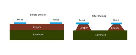
What is PCB Etching?
PCB etching is the process of removing unwanted copper from a copper-clad laminate to create the desired circuit pattern. In multilayer PCBs, etching is performed on the inner layers before they are laminated together with insulating prepreg materials to form the complete board Stackup.
The etching process involves the following key steps:
-
Applying a photoresist: A light-sensitive polymer coating, called photoresist, is applied to the copper surface of the inner layer. This photoresist will protect the copper that will form the final circuit traces.
-
Exposing the photoresist: The photoresist-coated inner layer is exposed to UV light through a photomask or phototool. The photomask contains the desired circuit pattern and blocks UV light from reaching the areas where copper should remain.
-
Developing the photoresist: After exposure, the inner layer is placed in a developing solution. This solution dissolves the unexposed portions of the photoresist, revealing the underlying copper that will be etched away.
-
Etching the copper: The developed inner layer is immersed in an etchant solution, typically cupric chloride or ammoniacal alkaline. The etchant chemically reacts with and removes the exposed copper, while the photoresist protects the desired copper traces.
-
Stripping the photoresist: Once etching is complete, the remaining photoresist is stripped away using a chemical stripper, leaving behind the etched copper circuit pattern on the inner layer.
Importance of Accurate Etching
Accurate and precise etching of inner layers is critical for several reasons:
-
Signal integrity: Properly etched traces ensure reliable signal transmission and minimize issues like crosstalk, impedance mismatch, and signal reflections.
-
Manufacturing yield: Consistent and accurate etching reduces the risk of defects and improves the overall manufacturing yield of PCBs.
-
Board reliability: Well-defined and cleanly etched traces contribute to the long-term reliability and durability of the PCB assembly.
-
Miniaturization: As electronic devices become smaller and more compact, precise etching enables the creation of fine-pitch traces and high-density interconnects.

Common PCB Etching Methods
There are several methods used for etching inner layers in PCB production. Each method has its advantages and limitations, and the choice depends on factors such as production volume, circuit complexity, and available resources.
Chemical Etching
Chemical etching is the most widely used method for PCB inner layer etching. It involves immersing the developed inner layer in an etchant solution that chemically dissolves the exposed copper. The two main types of chemical etchants are:
-
Acidic etchants: Cupric chloride (CuCl₂) is the most common acidic etchant. It offers fast etch rates and good selectivity but requires careful control of parameters like temperature, pH, and chloride ion concentration.
-
Alkaline etchants: Ammoniacal alkaline etchants, such as ammonium persulfate ((NH₄)₂S₂O₈), provide a safer and more environmentally friendly alternative to acidic etchants. They offer excellent etch uniformity and compatibility with various photoresists but have slower etch rates compared to acidic etchants.
Chemical etching is performed in conveyorized or batch etching systems, depending on production volume and throughput requirements.
Plasma Etching
Plasma etching, also known as dry etching, uses a plasma (ionized gas) to remove the exposed copper from the inner layer. The process takes place in a vacuum chamber, where a high-frequency electromagnetic field ionizes a gas (usually a mixture of chlorine and argon) to create a plasma.
The plasma contains highly reactive species that chemically react with and etch away the exposed copper. Plasma etching offers several advantages over chemical etching:
-
Anisotropic etching: Plasma etching can produce highly anisotropic (directional) etch profiles, enabling the creation of fine-pitch traces and high-density interconnects.
-
Reduced undercut: The anisotropic nature of plasma etching minimizes undercut, resulting in more precise and well-defined trace geometries.
-
Dry process: Plasma etching is a dry process, eliminating the need for handling and disposing of liquid etchants.
However, plasma etching has some limitations, such as higher equipment costs, slower etch rates, and potential plasma-induced damage to the substrate or photoresist.
Laser Etching
Laser etching uses a high-powered laser to selectively remove the exposed copper from the inner layer. The laser beam is focused onto the copper surface and scanned across the areas to be etched. The intense heat generated by the laser vaporizes the copper, leaving behind the desired circuit pattern.
Laser etching offers several advantages:
-
High precision: Laser etching can produce extremely fine and precise trace geometries, making it suitable for high-density PCB designs.
-
Rapid processing: Laser etching can be performed at high speeds, enabling faster turnaround times and increased production throughput.
-
Environmentally friendly: Laser etching is a dry process and does not require the use of chemical etchants, reducing environmental impact.
However, laser etching has some limitations, such as high equipment costs, potential thermal damage to the substrate, and the need for specialized laser-compatible photoresists.

Factors Affecting Etch Quality
Several factors can influence the quality and consistency of inner layer etching. Understanding and controlling these factors is essential for achieving optimal etch results.
Photoresist Quality
The quality of the photoresist plays a crucial role in determining the final etch quality. A high-quality photoresist should have the following characteristics:
-
Good adhesion: The photoresist must adhere well to the copper surface to prevent etchant undercutting and maintain trace integrity.
-
High resolution: The photoresist should be capable of resolving fine features and geometries to enable the creation of dense circuit patterns.
-
Chemical resistance: The photoresist must withstand the etching process without degrading or losing its protective properties.
Exposure and Development
Proper exposure and development of the photoresist are critical for achieving accurate etch patterns. Factors to consider include:
-
Exposure dose: The exposure dose (intensity and duration) must be optimized to ensure complete crosslinking of the photoresist in the exposed areas.
-
Alignment: Precise alignment of the photomask or phototool to the inner layer is essential for maintaining trace position and geometry.
-
Development time: The development time must be carefully controlled to ensure complete removal of the unexposed photoresist without overdeveloping and compromising trace width.
Etchant Composition and Control
The composition and control of the etchant solution are critical factors in achieving consistent and high-quality etching.
For chemical etching, the following parameters must be monitored and maintained within specified ranges:
-
Etchant concentration: The concentration of the active etchant species (e.g., cupric ions in acidic etchants) must be kept within the recommended range to ensure optimal etch rates and uniformity.
-
pH: The pH of the etchant solution must be controlled to maintain the desired etch rate and prevent unwanted side reactions.
-
Temperature: The temperature of the etchant solution must be maintained within the specified range to ensure consistent etch rates and prevent photoresist degradation.
For plasma etching, key parameters include gas composition, flow rate, pressure, and RF power. These parameters must be optimized to achieve the desired etch rate, selectivity, and anisotropy.
Etch Rate and Uniformity
Etch rate and uniformity are critical factors in achieving consistent and reliable etching results. Factors that can affect etch rate and uniformity include:
-
Agitation: Proper agitation of the etchant solution ensures uniform etchant distribution and prevents localized etchant depletion, resulting in more consistent etch rates across the panel.
-
Panel loading: The number and spacing of panels in the etching system can affect etch uniformity. Overloading the system can lead to etchant depletion and reduced etch rates in certain areas.
-
Etchant replenishment: Regular replenishment of the etchant solution is necessary to maintain consistent etch rates and prevent the build-up of etch byproducts that can compromise etch quality.

Best Practices for Optimal Inner Layer Etching
To achieve the best results in inner layer etching, consider the following best practices:
-
Use high-quality materials: Choose high-quality copper-clad laminates, photoresists, and etchants to ensure consistent and reliable etching performance.
-
Optimize exposure and development: Fine-tune exposure and development parameters to achieve crisp and well-defined trace geometries.
-
Monitor and control etchant parameters: Regularly monitor and adjust etchant composition, pH, temperature, and other critical parameters to maintain consistent etch rates and uniformity.
-
Implement proper agitation: Ensure adequate and uniform agitation of the etchant solution to promote even etching and prevent localized etchant depletion.
-
Maintain equipment: Regularly maintain and calibrate etching equipment to ensure optimal performance and minimize the risk of defects.
-
Use appropriate etch compensation: Incorporate etch compensation in the PCB design to account for the expected amount of lateral etching and maintain the desired trace widths.
-
Implement quality control measures: Establish a robust quality control process that includes regular inspections, measurements, and tests to verify etch quality and catch any issues early in the production process.
Frequently Asked Questions (FAQ)
1. What is the difference between inner layer and outer layer etching in PCB production?
Inner layer etching is performed on the copper layers that are sandwiched between the insulating layers of a multilayer PCB, while outer layer etching is performed on the top and bottom copper layers of the board. Inner layer etching is typically done before the layers are laminated together, while outer layer etching is done after lamination and drilling.
2. Can different etching methods be used for different layers in the same PCB?
Yes, it is possible to use different etching methods for different layers in the same PCB. For example, a manufacturer may choose to use chemical etching for the inner layers and plasma etching for the outer layers to achieve the desired trace geometries and densities.
3. How does the choice of copper thickness affect the etching process?
The copper thickness of the inner layers can affect the etching process in several ways. Thicker copper layers require longer etch times and may be more susceptible to undercut and trace width variation. Thinner copper layers etch faster but may be more vulnerable to over-etching and trace damage. The choice of copper thickness should be based on the specific design requirements and manufacturing capabilities.
4. What environmental considerations are involved in PCB etching?
PCB etching, particularly chemical etching, can have significant environmental impacts. Etchants and rinse waters contain heavy metals and other toxic substances that must be properly treated and disposed of to prevent pollution. Manufacturers must comply with local environmental regulations and implement appropriate waste management and treatment systems. Alternative etching methods, such as plasma etching, can help reduce the environmental footprint of PCB production.
5. How can PCB designers ensure their designs are optimized for etching?
PCB designers can optimize their designs for etching by following best practices such as:
- Using appropriate trace widths and spacing based on the etching method and capabilities.
- Incorporating etch compensation in the design to account for lateral etching.
- Avoiding acute angles and using teardrop pads to prevent over-etching and trace damage.
- Using symmetrical and balanced copper distribution to promote even etching and prevent panel warpage.
- Communicating with the manufacturer to understand their specific etching requirements and guidelines.
By designing with etching in mind, PCB designers can help ensure the manufacturability and reliability of their boards.
Conclusion
Etching inner layers is a critical step in the production of multilayer PCBs. The accuracy, precision, and consistency of the etching process directly impact the quality, reliability, and performance of the final PCB assembly. By understanding the different etching methods, factors affecting etch quality, and best practices for optimal results, PCB designers and manufacturers can work together to create high-quality boards that meet the demands of modern electronic devices.
As PCB technology continues to evolve, with increasing complexity, higher densities, and more stringent performance requirements, the importance of effective inner layer etching will only grow. Staying up-to-date with the latest advancements in etching processes, materials, and equipment will be essential for maintaining a competitive edge in the fast-paced world of PCB production.
No responses yet