Introduction to PCB Layers
Printed Circuit Boards (PCBs) are the backbone of modern electronics. They are used in almost every electronic device, from smartphones and laptops to industrial equipment and medical devices. PCBs are made up of multiple layers of conductive and insulating materials, each serving a specific purpose. Understanding the different types of PCB layers and their functions is crucial for designing and manufacturing reliable and efficient electronic products.
In this article, we will dive deep into the world of PCB layers, exploring their types, characteristics, and applications. We will also discuss the importance of choosing the right number and configuration of layers for your project, as well as some best practices for PCB layer stackup design.
What are PCB Layers?
PCB layers are the different levels of conductive and insulating materials that make up a printed circuit board. Each layer serves a specific purpose, such as providing electrical connections, insulation, or mechanical support. The number of layers in a PCB can vary depending on the complexity and requirements of the circuit design.
Types of PCB Layers
There are several types of PCB layers, each with its own characteristics and functions. The most common types of PCB layers include:
-
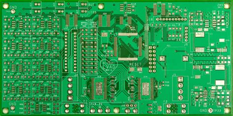
Copper Layers: These are the conductive layers that carry electrical signals and power throughout the PCB. Copper layers are typically made of a thin layer of copper foil laminated onto an insulating substrate. The thickness of the copper layer is measured in ounces per square foot (oz/ft²), with common thicknesses ranging from 0.5 oz/ft² to 2 oz/ft².
-
Substrate Layers: These are the insulating layers that provide mechanical support and electrical insulation between the copper layers. Substrate layers are typically made of materials such as FR-4, which is a glass-reinforced epoxy laminate. The thickness of the substrate layer is measured in thousands of an inch (mils), with common thicknesses ranging from 0.005″ to 0.062″.
-
Solder Mask Layers: These are the protective layers that cover the copper traces on the outer layers of the PCB, leaving only the exposed pads and vias for soldering. Solder mask layers are typically made of a polymer material that is applied as a liquid and then cured. The color of the solder mask can vary, with green being the most common.
-
Silkscreen Layers: These are the layers that contain text, symbols, and logos printed on the outer layers of the PCB for identification and assembly purposes. Silkscreen layers are typically made of a polymer material that is applied as a liquid and then cured. The color of the silkscreen can vary, with white being the most common.
Number of Layers in a PCB
The number of layers in a PCB can vary depending on the complexity and requirements of the circuit design. The most common PCB layer configurations are:
| Number of Layers | Description |
|---|---|
| Single Layer | A PCB with only one copper layer, typically used for simple circuits and low-cost applications. |
| Double Layer | A PCB with two copper layers, one on each side of the substrate, typically used for more complex circuits and higher-density applications. |
| Multi-Layer | A PCB with three or more copper layers, alternating with insulating substrate layers, typically used for very complex circuits and high-speed applications. |
The choice of the number of layers in a PCB depends on several factors, such as:
- Circuit complexity and density
- Signal integrity and electromagnetic compatibility (EMC) requirements
- Power distribution and thermal management needs
- Manufacturing cost and lead time constraints
In general, adding more layers to a PCB increases its complexity, cost, and manufacturing time, but also provides more flexibility and performance for the circuit design.

PCB Layer Stackup Design
PCB layer stackup design is the process of arranging the different layers of a PCB in a specific order and configuration to achieve the desired electrical, mechanical, and thermal performance. The layer stackup design is a critical aspect of PCB design, as it affects the signal integrity, power distribution, and manufacturability of the board.
Factors to Consider in PCB Layer Stackup Design
When designing a PCB layer stackup, there are several factors to consider, such as:
-
Signal Integrity: The layer stackup should be designed to minimize signal distortion, crosstalk, and electromagnetic interference (EMI) between the different layers and signals. This can be achieved by proper spacing and shielding of the signal layers, as well as the use of controlled impedance traces and ground planes.
-
Power Distribution: The layer stackup should be designed to provide adequate power distribution and decoupling for the different components and circuits on the board. This can be achieved by the use of dedicated power and ground planes, as well as the proper placement and sizing of decoupling capacitors.
-
Thermal Management: The layer stackup should be designed to provide efficient heat dissipation and thermal management for the components and circuits on the board. This can be achieved by the use of thermal vias, heat spreaders, and proper spacing and ventilation of the layers.
-
Manufacturing Constraints: The layer stackup should be designed to meet the manufacturing capabilities and constraints of the PCB fabricator, such as minimum trace width and spacing, drill sizes, and material availability. This can be achieved by close collaboration and communication with the PCB fabricator throughout the design process.
Best Practices for PCB Layer Stackup Design
Here are some best practices for designing a robust and reliable PCB layer stackup:
-
Use even number of layers: Using an even number of layers in the stackup helps to balance the mechanical stresses and prevent warping of the board during manufacturing and assembly.
-
Use symmetrical stackup: Using a symmetrical layer stackup, where the layers are mirrored around the center of the board, helps to minimize the differences in thermal expansion and mechanical stresses between the layers.
-
Use dedicated power and ground planes: Using dedicated power and ground planes in the stackup helps to provide a low-impedance path for the power and return currents, as well as to shield the signal layers from EMI.
-
Use controlled impedance traces: Using controlled impedance traces in the signal layers helps to match the impedance of the traces to the source and load impedances, and to minimize signal reflections and distortions.
-
Use appropriate spacing and shielding: Using appropriate spacing and shielding between the different layers and signals helps to minimize crosstalk and EMI, and to ensure signal integrity and reliability.

PCB Layer Materials
The choice of materials for the different layers of a PCB is another critical aspect of PCB design, as it affects the electrical, mechanical, and thermal properties of the board. The most common materials used in PCB layers are:
Copper
Copper is the most widely used material for the conductive layers of a PCB, due to its excellent electrical conductivity, thermal conductivity, and mechanical strength. Copper foils are available in different thicknesses and grades, depending on the application and requirements of the PCB.
FR-4
FR-4 is the most common material used for the insulating substrate layers of a PCB, due to its good electrical insulation, mechanical strength, and thermal stability. FR-4 is a composite material made of woven fiberglass cloth impregnated with an epoxy resin. FR-4 is available in different thicknesses and grades, depending on the application and requirements of the PCB.
Other Materials
Other materials used in PCB layers include:
| Material | Description |
|---|---|
| Polyimide | A high-temperature, flexible insulating material used for flex and Rigid-Flex PCBs. |
| PTFE | A low-dielectric, low-loss insulating material used for high-frequency and Microwave PCBs. |
| Aluminum | A metal substrate material used for high-power and high-thermal-conductivity PCBs. |
| Ceramic | A high-temperature, high-strength insulating material used for high-reliability and High-Voltage PCBs. |
The choice of materials for the PCB layers depends on several factors, such as:
- Electrical properties (dielectric constant, loss tangent, breakdown voltage)
- Thermal properties (glass transition temperature, thermal conductivity, coefficient of thermal expansion)
- Mechanical properties (strength, stiffness, flexibility, dimensional stability)
- Environmental properties (moisture absorption, flammability, chemical resistance)
- Cost and availability

PCB Layer Manufacturing Processes
The manufacturing of PCB layers involves several processes, each with its own challenges and requirements. The most common PCB layer manufacturing processes are:
Lamination
Lamination is the process of bonding the different layers of the PCB together using heat and pressure. The layers are stacked in the desired order and configuration, with the copper foils and prepreg (pre-impregnated) sheets in between. The stack is then placed in a lamination press, where it is heated and pressed at a specific temperature and pressure for a specific time, depending on the material and thickness of the layers.
Drilling
Drilling is the process of creating holes in the PCB for the component leads, vias, and mounting holes. The drilling is typically done using computer numerical control (CNC) machines, which use high-speed drill bits to create the holes in the desired locations and sizes. The drilling process is critical for the accuracy and reliability of the PCB, as it affects the alignment and connectivity of the layers.
Plating
Plating is the process of depositing a thin layer of metal (usually copper) on the walls of the drilled holes and on the surface of the outer layers of the PCB. The plating is typically done using electroplating or electroless plating techniques, which use an electric current or a chemical reaction to deposit the metal on the surface. The plating process is critical for the electrical connectivity and mechanical strength of the PCB, as it provides a conductive path between the layers and a protective coating on the surface.
Etching
Etching is the process of removing the unwanted copper from the surface of the PCB, leaving only the desired circuit pattern. The etching is typically done using a chemical etching process, which uses an acidic or alkaline solution to dissolve the copper in the areas not protected by the etch resist. The etching process is critical for the accuracy and resolution of the circuit pattern, as it defines the traces, pads, and planes of the PCB.
Solder Mask and Silkscreen
Solder mask and silkscreen are the processes of applying the protective and identification layers on the outer surfaces of the PCB. The solder mask is typically applied as a liquid photoimageable polymer, which is exposed and developed to create the openings for the pads and vias. The silkscreen is typically applied as a liquid epoxy ink, which is screen printed on the surface with the desired text, symbols, and logos. The solder mask and silkscreen processes are critical for the protection and identification of the PCB, as they prevent solder bridging and provide visual references for assembly and testing.
PCB Layer Design Tools
Designing a PCB layer stackup and layout requires the use of specialized software tools that can handle the complexity and constraints of the circuit design. Some of the most popular PCB layer design tools are:
Altium Designer
Altium Designer is a powerful and integrated PCB design tool that provides a complete solution for schematic capture, PCB layout, and manufacturing output. Altium Designer has a user-friendly interface and a rich set of features for PCB layer stackup design, such as automatic layer management, impedance calculation, and 3D visualization.
Cadence Allegro PCB Designer
Cadence Allegro PCB Designer is a high-end PCB design tool that provides advanced capabilities for PCB layout, routing, and manufacturing output. Allegro PCB Designer has a flexible and customizable interface and a comprehensive set of features for PCB layer stackup design, such as constraint-driven layout, signal integrity analysis, and thermal simulation.
KiCad EDA
KiCad EDA is a free and open-source PCB design tool that provides a complete solution for schematic capture, PCB layout, and manufacturing output. KiCad EDA has a modular and extensible architecture and a growing community of users and developers. KiCad EDA has a basic set of features for PCB layer stackup design, such as layer management, design rule checking, and 3D rendering.
Eagle PCB
Eagle PCB is a popular and affordable PCB design tool that provides a streamlined solution for schematic capture, PCB layout, and manufacturing output. Eagle PCB has a simple and intuitive interface and a limited set of features for PCB layer stackup design, such as layer stacking, drill optimization, and Gerber output.
The choice of PCB layer design tool depends on several factors, such as:
- Design complexity and requirements
- User experience and preferences
- Integration with other tools and workflows
- Budget and licensing options
Conclusion
PCB layers are the building blocks of modern electronics, providing the electrical, mechanical, and thermal infrastructure for the components and circuits on the board. Understanding the types, characteristics, and applications of PCB layers is essential for designing and manufacturing reliable and efficient electronic products.
Designing a PCB layer stackup and layout requires careful consideration of the signal integrity, power distribution, thermal management, and manufacturing constraints of the board. Following best practices and using appropriate materials and manufacturing processes can help ensure the quality and reliability of the PCB.
Using specialized PCB layer design tools can help streamline the design process and optimize the performance and manufacturability of the board. Choosing the right tool depends on the specific needs and resources of the project and the designer.
FAQ
- What is the difference between a single-layer and a multi-layer PCB?
-
A single-layer PCB has only one conductive layer, typically used for simple circuits and low-cost applications. A multi-layer PCB has three or more conductive layers, alternating with insulating layers, typically used for complex circuits and high-density applications.
-
What is the purpose of the solder mask layer on a PCB?
-
The solder mask layer is a protective layer that covers the copper traces on the outer layers of the PCB, leaving only the exposed pads and vias for soldering. The solder mask layer helps prevent solder bridging and provides insulation and protection for the copper traces.
-
What is the difference between FR-4 and Polyimide PCB materials?
-
FR-4 is a common PCB material made of woven fiberglass cloth impregnated with an epoxy resin, providing good electrical insulation, mechanical strength, and thermal stability. Polyimide is a high-temperature, flexible PCB material used for flex and rigid-flex PCBs, providing better flexibility and thermal resistance than FR-4.
-
What is the purpose of controlled impedance traces in a PCB?
-
Controlled impedance traces are used in the signal layers of a PCB to match the impedance of the traces to the source and load impedances, and to minimize signal reflections and distortions. Controlled impedance traces help ensure signal integrity and reliability, especially for high-speed and high-frequency applications.
-
What are the advantages of using a symmetrical PCB layer stackup?
- Using a symmetrical PCB layer stackup, where the layers are mirrored around the center of the board, helps to balance the mechanical stresses and prevent warping of the board during manufacturing and assembly. A symmetrical stackup also helps to minimize the differences in thermal expansion and signal propagation between the layers, improving the reliability and performance of the PCB.
No responses yet