Introduction to PCB Layers
Printed Circuit Boards (PCBs) are the backbone of modern electronics. They provide a platform for electronic components to be mounted and connected, forming a complete circuit. One of the key decisions in PCB design is choosing between a single layer or double layer PCB. In this article, we will explore the differences between these two types of PCBs, their advantages and disadvantages, and help you determine which one is best suited for your project.
What are PCB Layers?
PCB layers refer to the number of conductive copper layers that make up the PCB. The most common types of PCBs are single layer and double layer.
-
Single Layer PCB: A single layer PCB has one layer of conductive copper on one side of the board. The components are mounted on the same side as the copper traces.
-
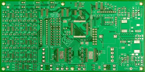
Double Layer PCB: A double layer PCB has two layers of conductive copper, one on each side of the board. The components can be mounted on both sides, and the layers are connected through vias (small holes filled with conductive material).
Advantages of Single Layer PCB
Cost-effective
Single layer PCBs are generally cheaper to manufacture compared to double layer PCBs. This is because they require fewer materials and less complex fabrication processes. If you have a simple circuit with a low component count, a single layer PCB can be a cost-effective solution.
Easier to Design
Designing a single layer PCB is relatively straightforward. Since all the components and traces are on one side, there is no need to worry about the placement of vias or the routing of traces between layers. This simplicity can lead to faster design times and fewer errors.
Suitable for Low-density Circuits
Single layer PCBs are ideal for low-density circuits with fewer components. If your project doesn’t require a large number of connections or complex routing, a single layer PCB can suffice.

Disadvantages of Single Layer PCB
Limited Routing Options
With only one layer of copper, the routing options on a single layer PCB are limited. As the number of components increases, it becomes more challenging to route traces without crossing or creating unintended connections. This limitation can lead to larger board sizes or compromises in the circuit design.
Higher Electromagnetic Interference (EMI)
Single layer PCBs are more susceptible to electromagnetic interference (EMI) compared to double layer PCBs. The lack of a ground plane on the opposite side of the board can result in increased noise and cross-talk between signals.
Limited Power Handling Capacity
The single layer of copper on a single layer PCB limits its power handling capacity. If your circuit requires high current or power dissipation, a single layer PCB may not be suitable.

Advantages of Double Layer PCB
Increased Routing Options
With two layers of copper, double layer PCBs offer more routing options. The additional layer allows for more complex routing and a higher density of components. Traces can be routed on both sides of the board, and vias can be used to connect signals between layers.
Better Signal Integrity
Double layer PCBs have better signal integrity compared to single layer PCBs. The ground plane on the opposite side of the board helps reduce electromagnetic interference and provides a stable reference for signals. This results in cleaner signals and reduced noise.
Higher Power Handling Capacity
The additional copper layer in a double layer PCB increases its power handling capacity. The extra layer can be used to create wider traces for high-current paths or to dissipate heat more effectively.
Smaller Board Size
With the increased routing options and higher component density, double layer PCBs can often be designed with a smaller board size compared to single layer PCBs. This can be advantageous in applications where space is limited.

Disadvantages of Double Layer PCB
Higher Cost
Double layer PCBs are more expensive to manufacture compared to single layer PCBs. The additional materials, fabrication steps, and complexity contribute to the higher cost. If your project has a tight budget, a double layer PCB may not be the most cost-effective choice.
More Complex Design Process
Designing a double layer PCB requires more effort and expertise compared to a single layer PCB. The placement of components, routing of traces, and use of vias need to be carefully considered to ensure proper functionality and manufacturability. This complexity can lead to longer design times and a higher possibility of errors.
Increased Manufacturing Time
The fabrication process for double layer PCBs is more involved compared to single layer PCBs. The additional steps, such as laminating the layers and drilling vias, can increase the manufacturing time. If your project has tight deadlines, this may be a consideration.
Choosing Between Single Layer and Double Layer PCB
When deciding between a single layer and double layer PCB, consider the following factors:
-
Circuit Complexity: If your circuit is simple with a low component count, a single layer PCB may suffice. However, if your circuit is more complex with a higher component density, a double layer PCB may be necessary.
-
Signal Integrity: If your circuit requires clean signals and low noise, a double layer PCB with a ground plane is recommended. Single layer PCBs are more susceptible to electromagnetic interference.
-
Power Handling: If your circuit demands high current or power dissipation, a double layer PCB with wider traces and better heat dissipation capabilities is preferred.
-
Board Size: Double layer PCBs can often achieve smaller board sizes compared to single layer PCBs due to the increased routing options and component density.
-
Cost: Single layer PCBs are generally cheaper to manufacture than double layer PCBs. Consider your project’s budget and the trade-offs between cost and performance.
-
Manufacturing Time: Double layer PCBs may have longer manufacturing times due to the additional fabrication steps involved.
| Factor | Single Layer PCB | Double Layer PCB |
|---|---|---|
| Circuit Complexity | Low | High |
| Signal Integrity | Lower | Higher |
| Power Handling | Limited | Better |
| Board Size | Larger | Smaller |
| Cost | Lower | Higher |
| Manufacturing Time | Shorter | Longer |
FAQ
-
Q: Can I use a single layer PCB for a high-speed digital circuit?
A: While it’s possible to use a single layer PCB for a high-speed digital circuit, it’s not recommended. High-speed signals are more susceptible to noise and interference, and a double layer PCB with a ground plane can provide better signal integrity. -
Q: Is it possible to have a mix of single layer and double layer PCBs in the same project?
A: Yes, it’s possible to have a mix of single layer and double layer PCBs in the same project. You can use single layer PCBs for simpler sub-circuits and double layer PCBs for more complex or sensitive parts of the design. -
Q: Can I convert a single layer PCB design to a double layer PCB?
A: Yes, you can convert a single layer PCB design to a double layer PCB. However, it may require some redesign and layout changes to optimize the use of the additional layer and ensure proper functionality. -
Q: Are there any limitations on the number of components that can be used on a single layer PCB?
A: There is no strict limitation on the number of components that can be used on a single layer PCB. However, as the component count increases, it becomes more challenging to route traces and maintain signal integrity. The practical limit depends on the size and complexity of the components and the available board space. -
Q: Can double layer PCBs be used for high-voltage applications?
A: Double layer PCBs can be used for high-voltage applications, but special considerations need to be taken. The PCB design must follow appropriate clearance and creepage distances, and the materials used should have suitable dielectric properties. It’s important to consult with PCB manufacturers and adhere to relevant safety standards when designing High-Voltage PCBs.
Conclusion
Choosing between a single layer and double layer PCB depends on various factors such as circuit complexity, signal integrity, power handling requirements, board size, cost, and manufacturing time. Single layer PCBs are cost-effective and suitable for simple, low-density circuits. Double layer PCBs offer increased routing options, better signal integrity, and higher power handling capacity, but come with higher costs and complexity.
When making the decision, carefully evaluate your project requirements and constraints. Consider the trade-offs between performance, cost, and manufacturing time. If your circuit demands clean signals, high power handling, or a compact board size, a double layer PCB may be the better choice. However, if you have a simple circuit with a low component count and budget constraints, a single layer PCB can be a viable option.
Ultimately, the choice between a single layer and double layer PCB should be based on a thorough analysis of your specific project needs. By understanding the advantages and disadvantages of each type and considering the key factors, you can make an informed decision that balances performance, cost, and manufacturability.
No responses yet