Step 1: Define Your Requirements
Before starting the design process, clearly define your requirements, including the operating frequency, power handling capability, signal integrity, and physical dimensions of the PCB.
Step 2: Choose the Right Substrate Material
Select a suitable substrate material based on your requirements. Common choices for Microwave PCBs include:
- Rogers RO4000 series
- Taconic TLY
- Isola IS680-280
- PTFE (Polytetrafluoroethylene)
Consider factors such as dielectric constant, dissipation factor, and thermal stability when choosing the substrate material.

Step 3: Determine the Layer Stack-up
Decide on the number of layers and their arrangement in the PCB Stack-up. A typical microwave PCB stack-up may include:
- Top layer: Signal and components
- Ground plane
- Dielectric substrate
- Bottom layer: Signal and components
Ensure proper spacing between layers to maintain signal integrity and minimize crosstalk.

Step 4: Calculate the Trace Width and Spacing
Calculate the appropriate trace width and spacing based on the operating frequency, characteristic impedance, and substrate properties. Use microwave transmission line calculators or simulation tools to determine the optimal values.
| Frequency (GHz) | Trace Width (mm) | Trace Spacing (mm) |
|---|---|---|
| 1-5 | 0.5-1.0 | 0.5-1.0 |
| 5-10 | 0.3-0.7 | 0.3-0.7 |
| 10-20 | 0.2-0.5 | 0.2-0.5 |

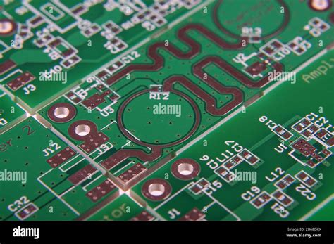
Step 5: Design the Microstrip or Stripline Transmission Lines
Choose between microstrip or stripline transmission lines based on your requirements. Microstrip lines are easier to fabricate but are more susceptible to radiation and coupling. Striplines offer better isolation but require more layers in the PCB stack-up.
Step 6: Implement Impedance Matching Techniques
Ensure proper impedance matching throughout the PCB to minimize reflections and signal distortions. Use techniques such as tapered lines, quarter-wave transformers, or stub matching to achieve the desired impedance.
Step 7: Minimize Discontinuities
Avoid abrupt discontinuities in the transmission lines, such as sharp bends or T-junctions. Use smooth transitions, chamfered corners, or mitered bends to minimize reflections and maintain signal integrity.
Step 8: Implement Grounding Techniques
Proper grounding is crucial in Microwave PCB Design. Use a solid ground plane and multiple vias to provide a low-impedance return path for the signals. Avoid slots or gaps in the ground plane that can cause unwanted resonances or coupling.
Step 9: Consider Electromagnetic Interference (EMI) Shielding
Incorporate EMI shielding techniques to minimize interference from external sources and reduce electromagnetic radiation from the PCB. Use shielding cans, conductive gaskets, or via fences around sensitive components or regions of the PCB.
Step 10: Place Components Strategically
Carefully place components on the PCB to minimize the length of high-frequency traces and reduce parasitic effects. Keep components close to their associated transmission lines and use surface-mount devices (SMDs) whenever possible.
Step 11: Route High-Frequency Signals Carefully
Route high-frequency signals on the top or bottom layer of the PCB to minimize the number of via transitions. Avoid routing signals over gaps or discontinuities in the ground plane, as this can lead to unwanted radiation or coupling.
Step 12: Implement Filters and Decoupling Capacitors
Use filters and decoupling capacitors to suppress unwanted harmonics, noise, and power supply fluctuations. Place decoupling capacitors close to the power pins of active components to provide a clean and stable power supply.
Step 13: Simulate and Optimize the Design
Perform electromagnetic simulations of your microwave PCB design using tools like Ansys HFSS, Keysight ADS, or Sonnet Software. Analyze the S-parameters, return loss, insertion loss, and radiation patterns to optimize the design for better performance.
Step 14: Consider Manufacturing Constraints
Collaborate with your PCB manufacturer to ensure that your design is compatible with their fabrication capabilities. Consider factors such as minimum trace width, spacing, via size, and hole diameter to avoid manufacturing issues.
Step 15: Perform Design Rule Checks (DRC)
Conduct thorough design rule checks to identify and resolve any violations of the PCB design guidelines. Check for issues such as insufficient clearances, trace width violations, or missing connections.
Step 16: Prototype and Test
Fabricate a prototype of your microwave PCB and perform rigorous testing to validate its performance. Measure the S-parameters, insertion loss, return loss, and power handling capabilities to ensure that the PCB meets your requirements.
Frequently Asked Questions (FAQ)
1. What is the difference between microstrip and stripline transmission lines?
Microstrip transmission lines are exposed on the top layer of the PCB, while striplines are embedded between two ground planes. Microstrip lines are easier to fabricate but are more susceptible to radiation and coupling. Striplines offer better isolation but require more layers in the PCB stack-up.
2. Why is impedance matching important in microwave PCB design?
Impedance matching is crucial to minimize reflections and signal distortions in microwave PCBs. Proper impedance matching ensures that the maximum amount of power is transferred from the source to the load, reducing signal loss and improving overall system performance.
3. How can I minimize electromagnetic interference (EMI) in my microwave PCB design?
To minimize EMI, you can implement shielding techniques such as using shielding cans, conductive gaskets, or via fences around sensitive components or regions of the PCB. Additionally, proper grounding and routing techniques can help reduce unwanted radiation and coupling.
4. What are some common substrate materials used for microwave PCBs?
Common substrate materials for microwave PCBs include Rogers RO4000 series, Taconic TLY, Isola IS680-280, and PTFE (Polytetrafluoroethylene). The choice of substrate material depends on factors such as dielectric constant, dissipation factor, and thermal stability.
5. Why is it important to collaborate with the PCB manufacturer during the design process?
Collaborating with the PCB manufacturer ensures that your design is compatible with their fabrication capabilities. This helps avoid manufacturing issues related to minimum trace width, spacing, via size, and hole diameter. Close collaboration can also lead to cost savings and faster turnaround times.
By following these 16 steps and considering the FAQ, you can design high-quality microwave PCBs that meet your requirements and perform optimally in your application.
No responses yet