Overview of PCB Manufacturing
Printed circuit board (PCB) manufacturing is the process of creating PCBs for use in electronic devices. The PCB acts as the foundation for the device, mechanically supporting and electrically connecting the components using conductive tracks, pads and other features.
PCB manufacturing can be divided into three main steps:
1. PCB Design & Engineering
2. PCB Fabrication
3. PCB Assembly
PCB Design & Engineering
The PCB manufacturing process begins with the design and engineering of the circuit board. This involves several sub-steps:
Schematic Diagram Creation
The first step is creating a schematic diagram that defines the electronic components and their connections. Engineers use electronic design automation (EDA) software to draw the schematic. Key information captured in the schematic includes:
- Component names, values, and part numbers
- Power and ground connections
- Component-to-component wiring
PCB Layout
With the schematic complete, the physical layout of the PCB is designed using EDA software. The PCB layout arranges the components and defines the copper traces that form the electrical connections between components. Important considerations during PCB layout include:
- Arranging components to minimize PCB size and maximize manufacturability
- Defining trace widths to carry the required current
- Ensuring traces are properly spaced to avoid unintended electrical shorts
- Adding planes for power and ground
- Defining any plated through-holes or vias
Design Rule Checks
The PCB layout undergoes design rule checks (DRC) to verify the design is manufacturable. DRC looks for violations of the PCB manufacturer’s capability, such as traces that are too close together or drill holes that are too small. Any issues are corrected before proceeding.
Gerber File Generation
Once the layout is finalized, Gerber files are generated from the EDA software. Gerber is the standard file format for defining the copper layers, solder mask, legend, and drill holes. The complete set of Gerber files fully describes the PCB design in a format that fabrication machines can use.

PCB Fabrication
With the Gerber files complete, the PCB is ready to be fabricated. PCB fabrication typically follows these steps:
Printing the Inner layers
For multi-layer PCBs, the inner layer copper patterns are printed onto special insulating base material. The circuit pattern is formed by applying a photoresist coating, then exposing to UV light through a photomask or film. Unexposed photoresist is chemically removed, then the exposed copper is etched away.
Aligning and Laminating Layers
The inner layers are stacked in the proper order with insulating prepreg material between each layer. Copper foil is placed on the top and bottom to form the outer layers. This stack-up is then laminated together under high heat and pressure in a forming press.
Drilling
Holes are drilled through the PCB Stack-up to allow electrical connections between layers. These drilled holes are called vias. High-speed drilling machines are used to quickly and accurately drill the vias.
Plating
The drilled PCB is then plated with copper to form the electrical connections from the inner layers to the outer layers. Additional copper is plated into the holes and on the outer layers to the desired thickness.
Outer Layer Patterning
Similar to the inner layer patterning process, the outer layer copper is patterned and etched. A photoresist coating is applied and exposed to define the desired copper pattern. The unexposed photoresist and unneeded copper are chemically removed.
Applying Solder Mask
A layer of polymer solder mask is applied to the outer layers of the PCB. The solder mask protects the copper traces from oxidation and prevents solder bridges from forming during assembly. Solder mask is typically green in color but other colors are available. Openings in the mask are left for component pads and vias.
Surface Finish
One of the final steps is to apply the surface finish to the exposed copper pads. The surface finish protects the copper and enhances solderability during assembly. Common surface finishes include:
| Surface Finish | Composition | Advantages |
|---|---|---|
| HASL | Tin-lead alloy | Low cost, good solderability |
| Lead-free HASL | Tin-copper alloy | RoHS compliant, good solderability |
| ENIG | Nickel/Gold | Flat surface, good shelf life |
| OSP | Organic coating | Low cost, good for fine-pitch devices |
Silkscreen
The top and bottom silkscreens are applied to the PCB. The silkscreen adds component outlines, reference designators, logos, and other markings to aid in assembly and identification. Silkscreen is most commonly white but other colors can be used.
Electrical Testing
As a final step, the fabricated PCB undergoes electrical testing to verify opens and shorts. Flying probe testers or bed-of-nails fixtures make contact with test points across the PCB to test for electrical continuity and isolation. Boards that fail are analyzed for manufacturing defects.

PCB Assembly
With fabrication complete, the PCB is ready for assembly. The main steps in assembly are:
Solder Paste Application
Solder paste, a mixture of tiny solder balls and flux, is applied to the component pads using a laser-cut stencil. The stencil is aligned to the PCB and solder paste is dispensed across the stencil surface, forcing paste through the holes onto the pads below.
Component Placement
The components are placed onto their pads by automated pick-and-place machines. These machines rapidly pick components from feeders and place them with high accuracy. Components may be glued in place for more challenging placements like fine-pitch BGAs.
Reflow Soldering
The PCB with placed components passes through a reflow oven on a conveyor belt. The oven has multiple heating zones that preheat, reflow the solder paste, and cool the assembly. The solder paste melts in the reflow zone, forming solder joints between the components and pads as it cools.
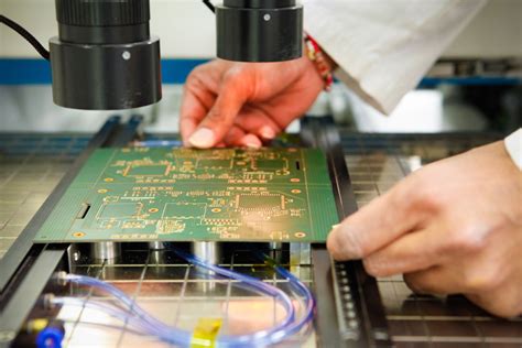
Inspection & Test
The assembled PCB undergoes automated optical inspection (AOI) to check for missed placements, rotated parts, and solder defects. Electrical tests also verify proper connectivity and functionality. Boards that fail inspection or test are reworked or scrapped.

Frequently Asked Questions
What is the typical turnaround time for PCB manufacturing?
Turnaround time varies based on the PCB complexity, quantity, and manufacturer capabilities. Simple 2-layer PCBs can be fabricated in 1-2 days while complex boards may take several weeks. Assembly requires additional time.
What are the most common PCB materials?
The base material is typically FR-4, a glass-reinforced epoxy laminate. Polyimide is used for flexible PCBs. High-frequency PCBs may use PTFE or Rogers materials for better electrical performance.
What are the standard copper weights?
Copper is specified in ounces per square foot, with 1 oz/ft² (35 µm) being the most common. Thinner ½ oz and thicker 2-3 oz copper are also frequently used depending on the current carrying and trace width requirements.
What is the minimum feature size for PCBs?
Standard PCB fabrication can achieve trace widths and spaces down to 3-4 mils (75-100 µm). High-density interconnect (HDI) processes can produce features as small as 1-2 mils (25-50 µm).
How are PCBs checked for quality?
Visual inspection, automated optical inspection (AOI), and X-ray are used to find manufacturing defects. Electrical testing verifies proper connectivity. Microsectioning is a destructive technique that cross-sections the PCB to inspect the plating and lamination quality.
I hope this guide provides a comprehensive overview of the PCB manufacturing process! Let me know if you have any other questions.
No responses yet