What is PCB 3D?
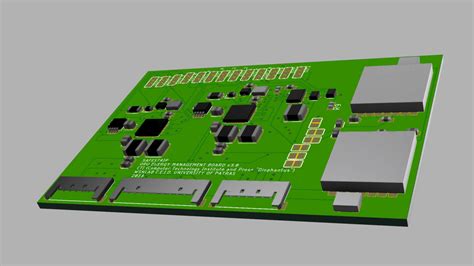
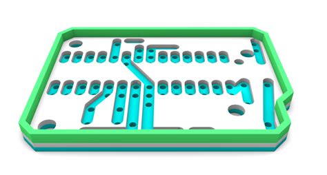
PCB 3D refers to the use of three-dimensional modeling and visualization techniques in the design of printed circuit boards. This approach allows designers to create a virtual representation of the PCB, including all its components, layers, and interconnections, in a 3D space. By using 3D modeling, designers can better understand the spatial relationships between different parts of the PCB and identify potential issues before the board is manufactured.
The Benefits of Using 3D Functions in PCB Design
1. Improved Visualization and Communication
One of the primary benefits of using 3D functions in PCB design is the improved visualization and communication it provides. With a 3D model, designers can easily visualize the placement of components, the routing of traces, and the overall layout of the board. This visual representation makes it easier for designers to communicate their ideas to other team members, such as mechanical engineers or manufacturing personnel, who may not be familiar with the intricacies of PCB design.
In addition, 3D models can be used to create realistic renderings of the final product, allowing stakeholders to see how the PCB will look and function in the real world. This can be particularly useful when presenting designs to clients or investors, as it provides a more tangible representation of the product than traditional 2D schematics.
2. Enhanced Design Accuracy and Efficiency
Another significant advantage of using 3D functions in PCB design is the enhanced accuracy and efficiency it offers. By working in a 3D environment, designers can more easily identify and resolve potential issues, such as component collisions, insufficient clearances, or Signal Integrity problems. This reduces the likelihood of errors and the need for costly redesigns later in the development process.
Moreover, 3D design tools often include automated features that can streamline the design process and improve efficiency. For example, some tools can automatically generate 3D models of components based on their 2D footprints, saving designers the time and effort of manually creating these models. Other tools may offer automated routing capabilities that can optimize the placement of traces and vias, reducing the risk of signal integrity issues and improving overall board performance.
3. Better Collaboration and Design Integration
PCB design often involves collaboration between multiple teams, such as electrical engineers, mechanical engineers, and manufacturing personnel. Using 3D functions in PCB design can facilitate better collaboration and design integration between these teams.
By sharing 3D models of the PCB, different teams can work together more effectively to ensure that the design meets all the necessary requirements. For example, mechanical engineers can use the 3D model to ensure that the PCB fits properly within the device enclosure and that there are no conflicts with other mechanical components. Similarly, manufacturing personnel can use the 3D model to assess the manufacturability of the design and provide feedback on potential improvements.
Furthermore, 3D design tools often include features that allow for the integration of PCB designs with other aspects of the product development process, such as mechanical design and thermal analysis. This integration enables a more holistic approach to product design, ensuring that all components work together seamlessly and that the final product meets all the necessary performance and reliability requirements.
4. Improved Signal Integrity and Electromagnetic Compatibility
Signal integrity and electromagnetic compatibility (EMC) are critical considerations in PCB design, particularly in high-speed and high-frequency applications. Using 3D functions in PCB design can help designers better address these issues and ensure the optimal performance of the board.
By creating a 3D model of the PCB, designers can more accurately simulate the behavior of signals as they propagate through the board. This allows them to identify potential signal integrity issues, such as crosstalk, reflections, or impedance mismatches, and take corrective actions to mitigate these problems. Additionally, 3D modeling can help designers optimize the placement and routing of components and traces to minimize electromagnetic interference (EMI) and ensure compliance with EMC standards.
Some 3D design tools also offer advanced simulation capabilities, such as full-wave electromagnetic simulation, which can provide even more accurate predictions of signal behavior and EMC performance. These simulations can help designers fine-tune their designs and ensure that the PCB will function as intended in the real world.
5. Cost Savings and Faster Time-to-Market
Ultimately, the use of 3D functions in PCB design can lead to significant cost savings and faster time-to-market for electronic products. By catching and resolving design issues early in the development process, designers can avoid costly redesigns and manufacturing delays. This not only saves money but also helps companies bring their products to market faster, giving them a competitive edge in today’s fast-paced technology landscape.
Moreover, the improved accuracy and efficiency offered by 3D design tools can help reduce the number of prototype iterations required, further cutting down on development time and costs. By getting the design right the first time, companies can minimize the need for expensive and time-consuming rework, allowing them to allocate their resources more effectively towards other aspects of product development.
Real-World Applications of PCB 3D Design
The use of 3D functions in PCB design has found widespread adoption across various industries, from consumer electronics to aerospace and defense. Here are a few examples of how PCB 3D design is being used in real-world applications:
-
Smartphones and Wearables: In the highly competitive world of consumer electronics, PCB 3D design has become essential for creating compact, high-performance devices. By using 3D modeling, designers can optimize the layout of components and traces to maximize space utilization and minimize signal integrity issues, enabling the development of ever-smaller and more powerful devices.
-
Automotive Electronics: As vehicles become increasingly reliant on electronic systems, the use of PCB 3D design has become crucial for ensuring the reliability and performance of these systems. By using 3D modeling to simulate the behavior of PCBs under various environmental conditions, such as temperature extremes and vibration, designers can create more robust and reliable electronic components for automotive applications.
-
Medical Devices: In the medical device industry, PCB 3D design is being used to create more compact and efficient devices that can improve patient outcomes and reduce healthcare costs. For example, by using 3D modeling to optimize the layout of a pacemaker PCB, designers can create a smaller, more reliable device that is less invasive and more comfortable for patients.
-
Aerospace and Defense: In the aerospace and defense industries, PCB 3D design is being used to create high-performance electronic systems that can withstand extreme environmental conditions and meet stringent reliability requirements. By using 3D modeling to simulate the behavior of PCBs under various stress factors, such as high altitudes and electromagnetic interference, designers can create more robust and reliable systems for mission-critical applications.

The Future of PCB 3D Design
As technology continues to advance, the use of 3D functions in PCB design is likely to become even more widespread and sophisticated. Here are a few trends and developments that are shaping the future of PCB 3D design:
-
Advanced Materials: The development of new, advanced materials, such as graphene and carbon nanotubes, is opening up new possibilities for PCB design. By using 3D modeling to simulate the behavior of these materials, designers can create PCBs with enhanced thermal, electrical, and mechanical properties, enabling the development of even more advanced electronic devices.
-
Artificial Intelligence and Machine Learning: The integration of artificial intelligence (AI) and machine learning (ML) technologies into PCB design tools is enabling more automated and intelligent design processes. By using AI and ML algorithms to analyze 3D models of PCBs, design tools can automatically identify potential issues and suggest optimizations, further improving the accuracy and efficiency of the design process.
-
Virtual and Augmented Reality: The use of virtual reality (VR) and augmented reality (AR) technologies in PCB design is providing designers with new ways to visualize and interact with their designs. By using VR and AR to create immersive 3D environments, designers can more easily collaborate with other team members and stakeholders, and gain a more intuitive understanding of the spatial relationships between different parts of the PCB.
-
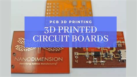
Additive Manufacturing: The rise of additive manufacturing, also known as 3D printing, is opening up new possibilities for PCB fabrication. By using 3D modeling to create printable PCB designs, designers can take advantage of the unique capabilities of additive manufacturing, such as the ability to create complex geometries and embedded components, enabling the development of more innovative and customized electronic devices.
Frequently Asked Questions (FAQ)
- What is the difference between 2D and 3D PCB Design?
-
2D PCB design involves creating a flat, two-dimensional representation of the PCB, focusing primarily on the placement and routing of components and traces. 3D PCB design, on the other hand, involves creating a three-dimensional model of the PCB, allowing designers to visualize and analyze the spatial relationships between different parts of the board.
-
What are the main benefits of using 3D functions in PCB design?
-
The main benefits of using 3D functions in PCB design include improved visualization and communication, enhanced design accuracy and efficiency, better collaboration and design integration, improved signal integrity and electromagnetic compatibility, and cost savings and faster time-to-market.
-
What industries are using PCB 3D design?
-
PCB 3D design is being used in a wide range of industries, including consumer electronics, automotive, medical devices, aerospace, and defense.
-
What are some of the trends shaping the future of PCB 3D design?
-
Some of the trends shaping the future of PCB 3D design include the development of advanced materials, the integration of artificial intelligence and machine learning technologies, the use of virtual and augmented reality, and the rise of additive manufacturing.
-
Do I need specialized skills or training to use 3D functions in PCB design?
- While using 3D functions in PCB design does require some specialized skills and training, many modern PCB design tools are becoming increasingly user-friendly and intuitive, making it easier for designers to adopt 3D design techniques. Additionally, there are many resources available, such as online tutorials and training courses, that can help designers learn the necessary skills to effectively use 3D functions in their work.
Conclusion
The use of 3D functions in PCB design has become an essential tool for creating efficient, reliable, and high-performance electronic devices. By providing improved visualization, enhanced accuracy, better collaboration, and faster time-to-market, 3D design techniques are enabling companies to stay competitive in today’s fast-paced technology landscape.
As technology continues to advance, the use of 3D functions in PCB design is likely to become even more widespread and sophisticated, with new developments in advanced materials, artificial intelligence, virtual reality, and additive manufacturing shaping the future of the field.
By embracing these new technologies and techniques, PCB Designers can create even more innovative and customized electronic devices that meet the evolving needs of consumers and businesses alike. As such, the use of 3D functions in PCB design is not just a trend, but a necessary evolution in the field of electronic design, one that will continue to drive progress and innovation for years to come.
No responses yet