Introduction to 3D PCB Design
In the world of electronics, Printed Circuit Boards (PCBs) play a crucial role in connecting and supporting electronic components. As technology advances and designs become more complex, the need for efficient and accurate PCB design methods has become more pressing. This is where 3D PCB design comes into play.
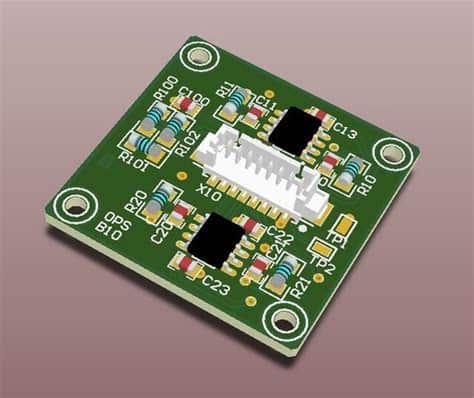
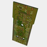
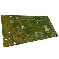
3D PCB design is a revolutionary approach to designing and visualizing PCBs in a three-dimensional space. It allows engineers and designers to create, manipulate, and analyze PCBs with greater precision and efficiency compared to traditional 2D design methods.
The Benefits of 3D PCB Design
Improved Visualization and Communication
One of the primary advantages of 3D PCB design is its ability to provide a clear and comprehensive visualization of the PCB. With 3D models, designers can easily understand the spatial relationships between components, traces, and layers. This enhanced visualization facilitates better communication among team members, manufacturers, and stakeholders.
Accurate Design and Error Reduction
3D PCB design tools allow for more accurate and precise design compared to 2D methods. By incorporating 3D models of components and enclosures, designers can ensure proper fit and clearance, reducing the likelihood of errors and design flaws. Additionally, 3D design software often includes automated design rule checks (DRC) and collision detection, helping to identify and resolve issues early in the design process.
Faster Prototyping and Time-to-Market
With 3D PCB design, the prototyping process becomes more efficient. Designers can create virtual prototypes and conduct simulations to test the functionality and performance of the PCB before physical fabrication. This allows for quick iterations and refinements, reducing the time and cost associated with physical prototyping.
Enhanced Collaboration and Data Management
3D PCB design tools often come with collaborative features that enable seamless teamwork and data management. Multiple designers can work on the same project simultaneously, with real-time updates and version control. This collaborative environment streamlines the design process, minimizes conflicts, and ensures that everyone is working with the most up-to-date information.
Key Features of 3D PCB Design Software
When considering 3D PCB design software, it’s important to look for key features that will enhance your design process. Some essential features include:
3D Modeling and Visualization
A robust 3D PCB design tool should provide advanced modeling and visualization capabilities. Look for software that supports the import and creation of 3D models for components, enclosures, and mechanical parts. The ability to view the PCB from different angles, zoom in and out, and apply realistic textures and colors will greatly aid in design comprehension and presentation.
Component Libraries and ECAD Integration
Having access to extensive component libraries is crucial for efficient PCB design. The software should offer a wide range of pre-built 3D models for common electronic components, as well as the ability to create custom models. Integration with Electronic Computer-Aided Design (ECAD) tools allows for seamless transfer of design data between electrical and mechanical domains.
Design Rule Checking (DRC) and Collision Detection
Automated design rule checking is a must-have feature in 3D PCB design software. DRC ensures that the design adheres to specified rules and constraints, such as minimum trace widths, clearances, and drill sizes. Collision detection helps identify any physical interferences between components, traces, and mechanical structures.
Thermal Analysis and Signal Integrity Simulation
Advanced 3D PCB design tools offer thermal analysis and signal integrity simulation capabilities. Thermal analysis allows designers to assess the heat distribution and identify potential thermal issues in the PCB. Signal integrity simulation helps analyze the behavior of high-speed signals and identify potential signal integrity problems, such as crosstalk and reflections.

Implementing 3D PCB Design in Your Workflow
Incorporating 3D PCB design into your existing workflow may seem daunting at first, but the benefits far outweigh the initial learning curve. Here are some steps to help you get started:
Evaluate and Select the Right Software
Research and evaluate different 3D PCB design software options based on your specific needs and budget. Consider factors such as ease of use, compatibility with your existing tools, and the availability of training and support resources.
Invest in Training and Education
To fully leverage the capabilities of 3D PCB design, invest in training and education for your team. Many software vendors offer training courses, tutorials, and webinars to help users get up to speed quickly. Encourage your team to explore online resources, attend conferences, and participate in user communities to stay updated on the latest trends and best practices.
Establish Design Standards and Guidelines
Develop a set of design standards and guidelines specific to 3D PCB design. These standards should cover aspects such as component placement, routing strategies, layer stackup, and mechanical considerations. Consistent adherence to these standards will ensure design quality and manufacturability.
Collaborate with Mechanical and Manufacturing Teams
3D PCB design facilitates better collaboration between electrical and mechanical teams. Engage with mechanical designers early in the design process to ensure proper integration of the PCB with the enclosure and other mechanical components. Work closely with manufacturing partners to validate the design for manufacturability and assembly.
Real-World Applications and Success Stories
3D PCB design has been successfully adopted across various industries, leading to significant improvements in product quality, time-to-market, and cost savings. Here are a few real-world examples:
Aerospace and Defense
In the aerospace and defense sector, 3D PCB design has revolutionized the development of high-reliability electronics. Companies have used 3D design tools to create complex, densely packed PCBs for avionics systems, satellite communications, and military equipment. The ability to visualize and simulate the PCB in a 3D environment has greatly reduced design errors and improved overall system reliability.
Automotive Electronics
The automotive industry has embraced 3D PCB design to keep pace with the increasing complexity of vehicle electronics. From infotainment systems to advanced driver assistance systems (ADAS), 3D design has enabled the development of compact, high-performance PCBs that can withstand the harsh automotive environment. Thermal analysis and signal integrity simulations have helped engineers optimize designs for reliability and performance.
Medical Devices
In the medical device industry, 3D PCB design has played a crucial role in the development of miniaturized, implantable devices. The ability to create accurate 3D models of the PCB and its enclosure has allowed designers to optimize the placement of components and ensure proper fit within the limited space available. 3D design has also facilitated the integration of sensors, antennas, and other specialized components in medical devices.
Frequently Asked Questions (FAQ)
1. What is the difference between 2D and 3D PCB design?
2D PCB design involves creating a flat, two-dimensional representation of the PCB, focusing on the placement of components and routing of traces. 3D PCB design, on the other hand, adds a third dimension to the design process, allowing designers to create and visualize the PCB in a three-dimensional space. 3D design incorporates the height and shape of components, as well as the mechanical aspects of the PCB and its enclosure.
2. Do I need specialized hardware for 3D PCB design?
While 3D PCB design software can be more demanding on computer resources compared to 2D tools, most modern computers with a dedicated graphics card and sufficient RAM can handle 3D design tasks. However, for complex and large-scale projects, it may be beneficial to invest in a high-performance workstation with a powerful CPU, GPU, and ample memory to ensure smooth and efficient design work.
3. How long does it take to learn 3D PCB design?
The learning curve for 3D PCB design depends on various factors, such as your prior experience with PCB design, familiarity with CAD tools, and the complexity of the software you choose. Generally, it may take a few weeks to a few months to become proficient in 3D PCB design, depending on the level of dedication and the availability of training resources. However, the long-term benefits of mastering 3D design far outweigh the initial time investment.
4. Can 3D PCB design files be used for manufacturing?
Yes, 3D PCB design files can be used for manufacturing. Most 3D PCB design software allows you to export the design data in various formats, such as Gerber files, ODB++, or IPC-2581, which are compatible with PCB fabrication and assembly processes. However, it’s important to communicate with your manufacturing partners to ensure that your design files meet their specific requirements and guidelines.
5. Is 3D PCB design suitable for all types of projects?
3D PCB design is beneficial for a wide range of projects, from simple boards to complex, high-density designs. However, the level of 3D design effort required may vary depending on the project’s complexity and requirements. For simpler projects with few components and straightforward layouts, a full-fledged 3D design approach may not be necessary. In such cases, a combination of 2D design with selective 3D modeling of critical components or areas can still provide significant benefits.
Conclusion
3D PCB design is a powerful tool that offers numerous benefits over traditional 2D design methods. From improved visualization and communication to accurate design and faster prototyping, 3D design empowers engineers and designers to create high-quality, reliable PCBs with greater efficiency.
By investing in the right 3D PCB design software, providing training and education for your team, and establishing design standards and guidelines, you can successfully integrate 3D design into your workflow. Collaborating closely with mechanical and manufacturing teams ensures a seamless design process and optimal results.
As technology continues to advance and product requirements become more demanding, 3D PCB design will play an increasingly crucial role in the development of innovative and reliable electronic products. Embracing this powerful design methodology will help you stay ahead of the curve and deliver exceptional results in today’s competitive market.
No responses yet