What are GERBER Files?
GERBER files, named after the Gerber Systems Corp., are a standard format used in the PCB industry to describe the layout and design of a PCB. They are essentially a set of vector-based images that represent the different layers of a PCB. Each layer is stored in a separate file with a specific extension that identifies its purpose. For example:
.gtl: Top copper layer.gbl: Bottom copper layer.gts: Top solder mask.gbs: Bottom solder mask.gto: Top silkscreen.gbo: Bottom silkscreen.txtor.drl: Drill data
These files are generated by PCB Design software and are used by PCB manufacturers to create the physical boards.
Why Reverse Generate PCB GERBER Files?
There are several reasons why you might need to reverse generate PCB GERBER files:
-
Legacy Designs: If you have an old PCB design that was created using software that is no longer available or supported, you may need to reverse engineer the GERBER files to update or modify the design using modern tools.
-
Obsolete Components: Sometimes, components used in a PCB design become obsolete or discontinued. In such cases, you may need to reverse engineer the GERBER files to identify the component footprints and find suitable replacements.
-
Troubleshooting: If you encounter issues with a manufactured PCB, reverse engineering the GERBER files can help you identify any design or manufacturing flaws that may be causing the problems.
-
Learning and Analysis: Reverse generating PCB GERBER files can be a valuable learning experience. By studying the design and layout of existing PCBs, you can gain insights into best practices, design techniques, and manufacturing considerations.
The Reverse Generation Process
Reverse generating PCB GERBER files involves several steps. Let’s explore each step in detail.
Step 1: Obtain the GERBER Files
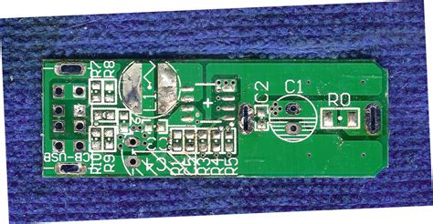
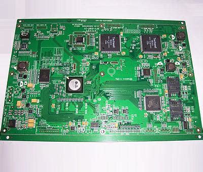
The first step is to acquire the GERBER files for the PCB you want to reverse engineer. If you have access to the original design files, you can simply export the GERBER files from the PCB design software. However, if you only have the physical PCB, you’ll need to use a scanner or a high-resolution camera to capture images of each layer.
Step 2: Convert Images to Vector Format
If you have scanned or photographed the PCB layers, you’ll need to convert the images into a vector format that can be edited and manipulated. This process is known as vectorization. There are several software tools available that can perform this task, such as:
- Adobe Illustrator
- Inkscape
- AutoTrace
- Vector Magic
These tools use algorithms to trace the bitmap images and convert them into vector paths and shapes.
Step 3: Clean Up and Organize the Vector Files
After vectorization, the resulting files may contain unwanted artifacts, stray lines, or incomplete shapes. It’s important to clean up these files to ensure accuracy and consistency. This can be done using vector editing software like Adobe Illustrator or Inkscape.
During this step, you should also organize the vector files into separate layers corresponding to the different PCB layers (copper, solder mask, silkscreen, etc.). This will make it easier to work with the files in the subsequent steps.
Step 4: Identify and Reconstruct Components
One of the most challenging aspects of reverse generating PCB GERBER files is identifying and reconstructing the components used in the design. This involves analyzing the copper traces, pads, and footprints to determine the type and size of each component.
You can use the following techniques to identify components:
- Visual Inspection: Carefully examine the PCB and compare the component footprints with known component packages and sizes.
- Reference Designs: Consult reference designs or datasheets for similar circuits to identify common components and their footprints.
- Online Resources: Utilize online resources such as component databases, forums, and communities dedicated to PCB design and reverse engineering.
Once you have identified the components, you need to reconstruct their footprints in the vector files. This may involve creating custom footprints or using pre-existing libraries.
Step 5: Reconstruct the Circuit Schematic
With the components identified and reconstructed, the next step is to reconstruct the circuit schematic. This involves tracing the copper traces and understanding how the components are interconnected.
You can use PCB design software or schematic capture tools to create a digital representation of the circuit. Start by placing the component symbols and then connecting them according to the traced copper traces. Pay attention to the signal flow, power and ground connections, and any special considerations such as shielding or Impedance matching.
Step 6: Verify and Validate the Design
After reconstructing the PCB design, it’s crucial to verify and validate its accuracy and functionality. This involves several checks:
- Design Rule Check (DRC): Perform a DRC to ensure that the reconstructed design adheres to the manufacturing and design rules specified by the PCB fabrication vendor.
- Electrical Rule Check (ERC): Conduct an ERC to verify that the reconstructed schematic is electrically correct and free from errors such as short circuits, open connections, or incorrect component polarities.
- Comparison with Original PCB: If possible, compare the reconstructed design with the original PCB to ensure that all components, traces, and features match.
- Prototype and Testing: If feasible, fabricate a prototype of the reconstructed PCB and perform thorough testing to validate its functionality and performance.
Step 7: Generate New GERBER Files
Once you have verified and validated the reconstructed PCB design, you can generate new GERBER files using the PCB design software. These files can then be used for manufacturing, modification, or further analysis.

Tools for Reverse Generating PCB GERBER Files
There are several software tools available that can assist in the process of reverse generating PCB GERBER files. Some popular options include:
| Tool | Description |
|---|---|
| KiCad | A free and open-source PCB design software suite that includes tools for reverse engineering. |
| Eagle | A widely used PCB design software with features for importing and editing GERBER files. |
| Altium Designer | A professional PCB design software with advanced capabilities for reverse engineering. |
| gerbv | An open-source GERBER file viewer that allows inspection and analysis of GERBER files. |
| Inkscape | A free vector graphics editor that can be used for vectorization and editing of PCB layers. |
| GerberLogix | A specialized software for analyzing, comparing, and reconstructing GERBER files. |
These tools offer different features and capabilities, and the choice depends on your specific requirements, budget, and expertise level.

Challenges and Considerations
Reverse generating PCB GERBER files comes with its own set of challenges and considerations. Some of the key challenges include:
-
Incomplete or Damaged Files: If the original GERBER files are incomplete, corrupted, or damaged, it can be difficult or impossible to accurately reconstruct the PCB design.
-
Complex Designs: Highly complex PCB designs with dense component placement, fine-pitch traces, or advanced manufacturing techniques can pose significant challenges during the reverse engineering process.
-
Intellectual Property: Reverse engineering a PCB design may raise intellectual property concerns. It’s important to ensure that you have the necessary rights and permissions to reverse engineer and use the reconstructed design.
-
Component Obsolescence: If the original PCB design uses obsolete or discontinued components, finding suitable replacements or recreating the exact footprints can be challenging.
-
Time and Effort: Reverse generating PCB GERBER files can be a time-consuming and labor-intensive process, especially for complex designs. It requires patience, attention to detail, and a systematic approach.
To overcome these challenges, it’s essential to have a well-defined process, use appropriate tools, and collaborate with experienced professionals when necessary.
FAQ
-
Q: Can I reverse generate PCB GERBER files from a physical PCB alone?
A: Yes, it is possible to reverse generate PCB GERBER files from a physical PCB by scanning or photographing each layer and then converting the images into vector format. However, having access to the original design files can simplify the process. -
Q: What if I encounter missing or damaged components during the reverse engineering process?
A: If you encounter missing or damaged components, you may need to rely on reference designs, datasheets, or expert knowledge to identify and recreate the missing components accurately. -
Q: How accurate are the reconstructed PCB designs compared to the original?
A: The accuracy of reconstructed PCB designs depends on various factors, such as the quality of the original files, the complexity of the design, and the skill of the person performing the reverse engineering. Thorough verification and validation processes can help ensure a high level of accuracy. -
Q: Can I use the reconstructed PCB design for commercial purposes?
A: The ability to use a reconstructed PCB design for commercial purposes depends on the intellectual property rights associated with the original design. It’s crucial to ensure that you have the necessary permissions and licenses before using or distributing the reconstructed design. -
Q: How long does it take to reverse generate PCB GERBER files?
A: The time required to reverse generate PCB GERBER files varies depending on the complexity of the design, the quality of the available files, and the experience of the person performing the task. Simple designs may take a few hours, while complex designs can take several days or even weeks.
Conclusion
Reverse generating PCB GERBER files is a valuable skill in the world of PCB design and manufacturing. Whether you need to update legacy designs, troubleshoot issues, or learn from existing PCBs, the ability to reconstruct designs from GERBER files is essential.
By following a systematic approach, using the right tools, and paying attention to detail, you can successfully reverse engineer PCB designs and generate new GERBER files for fabrication or further analysis. However, it’s important to be aware of the challenges and considerations involved, such as intellectual property rights, component obsolescence, and the time and effort required.
With the knowledge and techniques outlined in this article, you can confidently embark on the process of reverse generating PCB GERBER files and unlock the insights hidden within PCB designs.
No responses yet