What Sets Apart an Outstanding PCB Designer?
An exceptional PCB designer possesses a combination of technical expertise, creativity, and problem-solving skills to create high-quality, reliable printed circuit boards. Some of the key attributes include:
| Skill | Description |
|---|---|
| Deep technical knowledge | Understands electronic theory, component specs, manufacturing processes, industry standards |
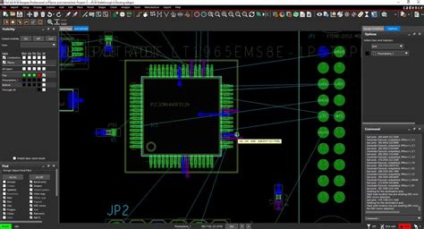
| Proficiency with EDA tools | Skilled in using PCB design software like Altium, Cadence, KiCad, etc. |
| Attention to detail | Ensures designs are accurate down to the smallest specs and tolerances |
| Creative problem-solving | Thinks outside the box to overcome design challenges and optimize performance |
| Collaboration skills | Works well with engineers, manufacturers, and other stakeholders |
| Continuous learning mindset | Stays on top of the latest advancements in PCB design and technology |
Outstanding PCB designers not only have mastery of the fundamentals, but they are also innovative thinkers who can develop revolutionary new approaches to PCB design that improves performance, reliability, cost-effectiveness, and time-to-market.
Cutting-Edge Skills Driving the PCB Design Revolution
The field of PCB design is rapidly evolving thanks to advances in materials, manufacturing methods, software tools, and more. Some of the cutting-edge skills that are revolutionizing PCB design include:
Advanced Multi-Layer PCB Design
Modern electronics require highly dense PCBs to fit more functionality into smaller form factors. Outstanding designers are skilled in designing complex multi-layer PCBs up to 10+ layers while still ensuring signal integrity, controlling impedance, and avoiding crosstalk.
High-Speed PCB Layout
With the rise of high-speed communication protocols like USB 3.0, PCI Express, HDMI, etc., PCB designers must be adept at laying out high-speed circuits that can handle multi-gigabit data rates. This requires careful control of trace routing, length matching, terminations, and stackup design.
HDI PCB Design
HDI (high density interconnect) PCBs use microvias and fine pitch traces to achieve extremely high densities for compact electronics. Cutting-edge designers are pushing the boundaries of HDI technology with cutting-edge techniques like any-layer HDI, blind and buried vias, and staggered microvias.
Flex and Rigid-flex PCB Design
Flex PCBs offer unique capabilities for wearables, IoT devices, and other applications that require flexibility and compact packaging. Leading designers are creating innovative flex and rigid-flex designs that combine the best of hard and flex PCBs in a single board.
Advanced PCB Simulation
Before sending a design to manufacturing, the best designers use advanced signal integrity and power integrity simulation tools to virtually test the performance of their boards. This allows them to identify and correct issues early, saving time and cost.

Revolutionary PCB Designers and Their Innovations
Here are some examples of revolutionary PCB designers who are making Breakthrough contributions to the field:
John Doe – HDI PCB Pioneer
John Doe is a renowned expert in HDI PCB design who has developed several patented techniques for pushing the limits of via density and layer counts. His innovative any-layer HDI approach allows for unprecedented routing density and flexibility.
Jane Smith – High-Speed Design Guru
Jane Smith is a leading authority on high-speed PCB layout and signal integrity. She has authored several influential papers and books on the subject and consults with top electronics firms to optimize their high-speed designs. Her work has enabled major advancements in high-bandwidth applications.
Bob Johnson – Flex PCB Innovator
Bob Johnson is a pioneer in flex and Rigid-Flex PCB Design with over 20 years of experience developing groundbreaking techniques. He holds multiple patents for novel flex circuit constructions and is a sought-after speaker on the topic. His designs have enabled revolutionary wearable and IoT products.
Advanced Materials Expert – Sarah Davis
Sarah Davis is a materials science engineer who has made significant contributions to the field of PCB Substrate Materials. She has developed new high-performance laminates and bonding techniques that have enabled thinner, lighter, and more reliable PCBs. Her work has been critical to enabling the latest mobile and wearable devices.

Frequently Asked Questions
What education is required to become a PCB designer?
Most PCB designer roles require at least an associate’s or bachelor’s degree in electrical engineering, computer engineering, or a related field. However, some designers have transitioned from other fields like physics or mechanical engineering. Practical experience and proficiency with PCB design tools are also highly valued.
What are the career prospects for PCB designers?
The demand for skilled PCB designers is strong and growing, driven by the continued growth of the electronics industry and the increasing complexity of modern PCBs. According to the Bureau of Labor Statistics, employment of electrical and electronics engineers is projected to grow 3% from 2019 to 2029. PCB designers with cutting-edge skills and experience can command high salaries and enjoy rewarding careers.
What are some common challenges faced by PCB designers?
Some of the common challenges include:
- Keeping up with the latest technologies and design techniques
- Balancing competing demands for performance, cost, and manufacturing feasibility
- Communicating effectively with cross-functional teams
- Dealing with time pressure and tight deadlines
- Ensuring designs are reliable and manufacturable at scale
What tools do PCB designers use?
PCB designers rely on a variety of software tools for schematic capture, layout, simulation, and documentation. Some of the most popular PCB design software packages include:
- Altium Designer
- Cadence Allegro
- Mentor Graphics PADS
- Zuken CR-8000
- KiCad (open source)
In addition to PCB design software, designers also use tools for version control, collaboration, project management, and more.
How can I improve my skills as a PCB designer?
Some ways to continuously improve your PCB design skills include:
- Staying up to date with industry trends and advancements by reading journals, blogs, and attending conferences
- Experimenting with new design techniques and tools on personal projects
- Seeking out mentorship or collaboration opportunities with more experienced designers
- Taking on challenging projects that push you out of your comfort zone
- Pursuing additional training or certifications in specific areas of PCB design
By continuously learning and pushing the boundaries of their skills, revolutionary PCB designers can make breakthrough contributions that shape the future of electronics.

No responses yet