Introduction to PCB Types
Printed Circuit Boards (PCBs) are essential components in modern electronics. They provide a platform for mounting and interconnecting electronic components, enabling the creation of complex circuits in a compact and efficient manner. PCBs come in various types, each with its own unique characteristics and applications. In this article, we will explore the different types of PCBs, their manufacturing processes, and their uses in various industries.
What is a PCB?
A Printed Circuit Board (PCB) is a flat board made of insulating material, typically fiberglass or composite epoxy, with conductive copper traces printed on its surface. These traces form the electrical connections between the various components mounted on the board. PCBs provide a stable and reliable platform for electronic circuits, allowing for high-density component placement and efficient signal routing.

PCB Manufacturing Process
The PCB manufacturing process involves several steps:
-
Design: The PCB layout is designed using specialized software, taking into account the component placement, signal routing, and manufacturing constraints.
-
Fabrication: The designed PCB is fabricated using a multi-step process that includes:
- Printing the copper traces on the insulating substrate
- Applying a photoresist layer and exposing it to UV light through a photomask
- Developing the photoresist to reveal the desired copper pattern
- Etching away the unwanted copper
- Drilling holes for component mounting and vias
-
Applying a solder mask and silkscreen for protection and labeling
-
Assembly: The fabricated PCB is populated with electronic components using various techniques, such as through-hole mounting or surface mount technology (SMT).
-
Testing: The assembled PCB undergoes rigorous testing to ensure proper functionality, reliability, and adherence to specifications.

Types of PCBs
PCBs can be categorized based on various factors, such as the number of layers, flexibility, and manufacturing technology. Let’s explore the different types of PCBs in detail.
1. Single-Sided PCB
Single-sided PCBs have conductive copper traces on only one side of the insulating substrate. They are the simplest and most cost-effective type of PCB. Single-sided PCBs are suitable for basic circuits with low component density and simple routing requirements. They are commonly used in low-cost consumer electronics, such as toys and simple appliances.
Advantages of Single-Sided PCBs
- Low manufacturing cost
- Simple design and fabrication process
- Suitable for basic circuits with few components
Disadvantages of Single-Sided PCBs
- Limited routing options due to single-sided copper traces
- Not suitable for high-density circuits or complex designs
- Prone to electromagnetic interference (EMI) and signal integrity issues
2. Double-Sided PCB
Double-sided PCBs have conductive copper traces on both sides of the insulating substrate. They offer increased routing options and higher component density compared to single-sided PCBs. Double-sided PCBs utilize through-hole vias to connect the traces on the top and bottom layers. They are commonly used in a wide range of applications, including consumer electronics, industrial equipment, and automotive systems.
Advantages of Double-Sided PCBs
- Increased routing options and component density
- Improved signal integrity and reduced EMI
- Suitable for more complex circuits and designs
Disadvantages of Double-Sided PCBs
- Higher manufacturing cost compared to single-sided PCBs
- More complex design and fabrication process
- Requires careful layer alignment and via placement
3. Multi-Layer PCB
Multi-layer PCBs consist of three or more conductive layers separated by insulating layers. They offer the highest level of routing options and component density among PCB types. Multi-layer PCBs utilize blind and buried vias to interconnect the layers, enabling complex signal routing and power distribution. They are commonly used in high-performance applications, such as aerospace, defense, and advanced telecommunications systems.
Advantages of Multi-Layer PCBs
- High routing density and component placement options
- Excellent signal integrity and reduced EMI
- Suitable for complex, high-speed, and high-frequency circuits
Disadvantages of Multi-Layer PCBs
- High manufacturing cost due to complex fabrication process
- Increased design complexity and longer development time
- Requires advanced manufacturing capabilities and expertise
| PCB Type | Layers | Routing Density | Cost | Applications |
|---|---|---|---|---|
| Single-Sided | 1 | Low | Low | Simple circuits, toys, basic appliances |
| Double-Sided | 2 | Medium | Medium | Consumer electronics, industrial equipment, automotive systems |
| Multi-Layer | 3+ | High | High | Aerospace, defense, advanced telecommunications |
4. Flexible PCB
Flexible PCBs (FPCBs) are made of thin, flexible insulating materials, such as polyimide or polyester, with conductive copper traces. They can bend and flex without damaging the circuit, making them ideal for applications that require conformity to non-planar surfaces or frequent flexing. FPCBs are commonly used in wearable devices, medical equipment, and aerospace applications.
Advantages of Flexible PCBs
- Conformity to non-planar surfaces and tight spaces
- Lightweight and thin profile
- High resistance to vibration and shock
- Reduced assembly time and cost
Disadvantages of Flexible PCBs
- Higher manufacturing cost compared to rigid PCBs
- Limited component mounting options due to flexibility
- Requires specialized design and manufacturing expertise
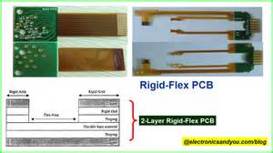
5. Rigid-flex PCB
Rigid-flex PCBs combine the benefits of both rigid and flexible PCBs. They consist of rigid PCB sections connected by flexible PCB sections, allowing for three-dimensional configurations and improved packaging density. Rigid-flex PCBs are commonly used in aerospace, defense, and medical devices, where high reliability and compact packaging are essential.
Advantages of Rigid-Flex PCBs
- Improved packaging density and space utilization
- Reduced interconnect complexity and assembly time
- High reliability and durability
- Suitable for three-dimensional configurations
Disadvantages of Rigid-Flex PCBs
- High manufacturing cost due to complex fabrication process
- Increased design complexity and development time
- Requires specialized manufacturing capabilities and expertise

PCB Materials
The choice of PCB material depends on various factors, such as the application requirements, operating environment, and cost considerations. Some common PCB materials include:
- FR-4: A fiberglass-reinforced epoxy laminate, widely used for general-purpose PCBs.
- High-Tg FR-4: A variant of FR-4 with improved thermal stability and higher glass transition temperature (Tg).
- Polyimide: A high-performance, heat-resistant material used for flexible PCBs and high-temperature applications.
- PTFE (Teflon): A low-dielectric constant material used for high-frequency and microwave applications.
- Aluminum: Used as a substrate for metal-core PCBs (MCPCBs) for improved heat dissipation.
PCB Applications
PCBs find applications in various industries, including:
- Consumer Electronics: Smartphones, tablets, laptops, televisions, and home appliances.
- Automotive: Engine control units, infotainment systems, and advanced driver assistance systems (ADAS).
- Industrial Automation: Programmable logic controllers (PLCs), sensors, and actuators.
- Medical Devices: Diagnostic equipment, monitoring systems, and implantable devices.
- Aerospace and Defense: Avionics, radar systems, and military communication equipment.
- Telecommunications: Networking equipment, base stations, and satellite communication systems.
Frequently Asked Questions (FAQ)
-
Q: What is the difference between a single-sided and double-sided PCB?
A: Single-sided PCBs have conductive copper traces on only one side of the insulating substrate, while double-sided PCBs have copper traces on both sides. Double-sided PCBs offer increased routing options and component density compared to single-sided PCBs. -
Q: What are the advantages of using a multi-layer PCB?
A: Multi-layer PCBs offer high routing density, excellent signal integrity, and reduced electromagnetic interference (EMI). They are suitable for complex, high-speed, and high-frequency circuits commonly found in advanced applications. -
Q: When should I consider using a flexible PCB?
A: Flexible PCBs are ideal for applications that require conformity to non-planar surfaces, frequent flexing, or tight packaging constraints. They are commonly used in wearable devices, medical equipment, and aerospace applications. -
Q: What factors should I consider when choosing a PCB material?
A: When choosing a PCB material, consider factors such as the application requirements, operating environment, thermal stability, dielectric properties, and cost. Common PCB materials include FR-4, high-Tg FR-4, polyimide, PTFE (Teflon), and aluminum. -
Q: What are the steps involved in the PCB manufacturing process?
A: The PCB manufacturing process typically involves four main steps: design, fabrication, assembly, and testing. The fabrication step includes printing the copper traces, applying photoresist, etching, drilling holes, and applying solder mask and silkscreen. Assembly involves populating the PCB with electronic components, and testing ensures proper functionality and reliability.
Conclusion
PCBs are essential components in modern electronics, providing a stable and reliable platform for interconnecting electronic components. The various types of PCBs, including single-sided, double-sided, multi-layer, flexible, and rigid-flex, offer different advantages and are suited for specific applications. Understanding the characteristics, manufacturing processes, and materials of each PCB type is crucial for designing and developing efficient and reliable electronic systems.
As technology advances and the demand for compact, high-performance electronics grows, PCBs will continue to evolve and play a vital role in shaping the future of electronics. By staying informed about the latest developments in PCB technology and manufacturing techniques, engineers and designers can create innovative solutions that push the boundaries of what is possible in the world of electronics.
No responses yet