Overview of the PCBA Manufacturing Process
The PCBA manufacturing process can be broadly divided into three main stages:
-
SMT (Surface Mount Technology) Placement: The surface mount components are placed and soldered onto the PCB.
-
THT (Through-Hole Technology) Placement: The through-hole components are inserted and soldered onto the PCB.
-
Inspection and Testing: The assembLED PCB undergoes various inspections and tests to ensure quality and functionality.
Let’s explore each of these stages in detail.
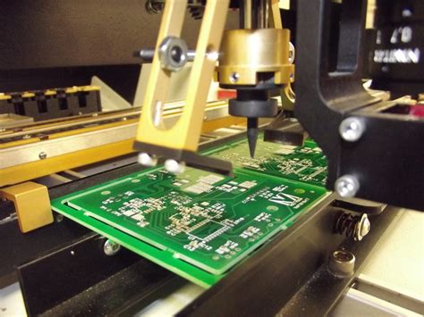
SMT (Surface Mount Technology) Placement
SMT is the more modern and widely used technology in PCBA manufacturing. It involves placing surface mount devices (SMDs) onto the surface of the PCB. SMDs are smaller and can be placed on both sides of the PCB, allowing for higher component density and smaller board sizes.
The SMT placement process involves several steps:
1. Solder Paste Printing
Solder paste, a mixture of tiny solder particles and flux, is applied to the PCB pads where the SMDs will be placed. This is typically done using a solder paste stencil and a screen printing machine.
2. SMD Placement
The SMDs are picked and placed onto the PCB by high-speed, high-precision pick-and-place machines. These machines use vacuum nozzles or grippers to pick up the components from feeders and place them accurately on the solder paste deposits.
3. Reflow Soldering
After SMD placement, the PCB goes through a reflow soldering process. The board is passed through a reflow oven, which heats it to a specific temperature profile. This melts the solder particles in the solder paste, creating a permanent bond between the component leads and the PCB pads.

THT (Through-Hole Technology) Placement
THT placement involves inserting the leads of through-hole components into holes drilled in the PCB and soldering them in place. Although THT is being gradually replaced by SMT, it is still used for certain components that are not available in SMT packages or for components that require higher mechanical strength.
The THT placement process involves two main steps:
1. Component Insertion
The leads of the through-hole components are inserted manually or by machine into the corresponding holes on the PCB.
2. Wave Soldering
The PCB with inserted components is passed over a molten solder wave. The solder adheres to the component leads and PCB holes, creating a strong mechanical and electrical bond.

Inspection and Testing
After the SMT and THT placement processes, the assembled PCB undergoes various inspections and tests to ensure quality and functionality.
1. Visual Inspection
A manual visual inspection is performed to check for any obvious defects, such as missing components, incorrect component placement, or solder bridging.
2. Automated Optical Inspection (AOI)
AOI uses high-resolution cameras and image processing software to automatically inspect the PCB for defects. It can detect issues such as missing components, incorrect polarity, and solder problems.
3. X-Ray Inspection
X-ray inspection is used to check for defects that are not visible to the naked eye or AOI, such as voids in solder joints or hidden solder balls.
4. In-Circuit Testing (ICT)
ICT is a type of electrical test that verifies the functionality of individual components and their interconnections on the PCB. It uses a bed-of-nails fixture to make contact with test points on the board and perform resistance, capacitance, and other measurements.
5. Functional Testing
Functional testing verifies the overall functionality of the assembled PCB. It involves powering up the board and running tests to ensure that it performs as intended.

Equipment and Materials Used in PCBA Manufacturing
The PCBA manufacturing process involves various specialized equipment and materials. Some of the key equipment and materials include:
| Equipment/Material | Description |
|---|---|
| Solder Paste Printer | Applies solder paste to PCB pads using a stencil |
| Pick-and-Place Machine | High-speed, high-precision machine for placing SMDs on the PCB |
| Reflow Oven | Heats the PCB to melt the solder paste and create a bond between components and pads |
| Wave Soldering Machine | Creates a solder wave for soldering through-hole components |
| AOI Machine | Automated optical inspection machine for detecting defects |
| X-Ray Machine | Used for inspecting hidden solder joints and defects |
| ICT Fixture | Bed-of-nails fixture for in-circuit testing |
| Solder Paste | A mixture of tiny solder particles and flux used for SMT soldering |
| Solder Wire | Used for manual soldering and rework |
| Flux | A chemical agent that helps to remove oxides and improve solder wettability |
Quality Control in PCBA Manufacturing
Quality control is critical in PCBA manufacturing to ensure that the assembled PCBs meet the required specifications and perform reliably. Some key aspects of quality control in PCBA manufacturing include:
1. Incoming Material Inspection
All incoming materials, including PCBs, components, and solder paste, are inspected to ensure that they meet the required specifications and are free from defects.
2. Process Control
The various processes in PCBA manufacturing, such as solder paste printing, SMD placement, and soldering, are closely monitored and controlled to ensure consistency and quality.
3. Traceability
Each PCB is assigned a unique identifier, and the manufacturing process is documented to ensure traceability. This allows for easier identification and resolution of any issues that may arise.
4. Employee Training
Employees involved in the PCBA manufacturing process are trained on the latest techniques, equipment, and quality standards to ensure consistent high-quality output.
Frequently Asked Questions (FAQ) about PCBA Manufacturing
- What is the difference between PCB and PCBA?
-
A PCB is a bare printed circuit board without any components. PCBA refers to a PCB with components assembled onto it.
-
What is the difference between SMT and THT?
-
SMT (Surface Mount Technology) involves placing components on the surface of the PCB, while THT (Through-Hole Technology) involves inserting component leads through holes in the PCB and soldering them in place.
-
What is the purpose of solder paste in SMT?
-
Solder paste, a mixture of tiny solder particles and flux, is used in SMT to temporarily hold the components in place before reflow soldering and to provide the solder for creating the electrical and mechanical bond between the component and the PCB.
-
What is the role of flux in soldering?
-
Flux is a chemical agent that removes oxides from the metal surfaces to be soldered and improves the wettability of the solder, ensuring a strong and reliable solder joint.
-
What are some common defects in PCBA manufacturing?
- Some common defects in PCBA manufacturing include missing components, incorrect component placement, solder bridging, Cold Solder Joints, and voids in solder joints. These defects can be detected through various inspection methods such as visual inspection, AOI, X-ray, and ICT.
Conclusion
The PCBA manufacturing process is a complex and precise process that involves multiple steps and specialized equipment. By understanding the various stages of the process, from SMT and THT placement to inspection and testing, and the key equipment and materials used, you can better appreciate the intricacies involved in creating the electronic devices we use every day.
Effective quality control measures, including incoming material inspection, process control, traceability, and employee training, are essential to ensure that the assembled PCBs meet the highest quality standards and perform reliably.
As technology continues to advance, the PCBA manufacturing process will also evolve, with new techniques and equipment being developed to meet the ever-increasing demand for smaller, more complex, and more reliable electronic devices.
No responses yet