Introduction to Via Filling
Via filling, also known as through-hole filling or via plating, is a crucial process in the manufacturing of printed circuit boards (PCBs). It involves the deposition of conductive material, usually copper, inside the drilled holes (vias) of a PCB to create electrical connections between different layers of the board. This process is essential for the proper functioning of multi-layer PCBs, as it ensures reliable electrical conductivity and signal integrity.
The Importance of Via Filling in PCB Manufacturing
Via filling plays a critical role in the performance and reliability of modern electronic devices. As the demand for smaller, more compact, and high-performance electronic products continues to grow, PCB Designers are faced with the challenge of incorporating more components and circuitry into limited space. This has led to the development of multi-layer PCBs, which rely heavily on via filling to establish electrical connections between layers.
Some of the key benefits of via filling include:
- Improved electrical conductivity
- Enhanced signal integrity
- Reduced electromagnetic interference (EMI)
- Better thermal management
- Increased mechanical strength
The Via Filling Process
The via filling process typically involves several steps, each of which contributes to the overall quality and reliability of the finished PCB. Here’s a detailed look at the various stages of via filling:
1. Drilling
The first step in via filling is drilling holes through the PCB substrate. This is done using specialized drilling machines that can create holes with precise diameters and locations. The size and placement of the holes depend on the specific design requirements of the PCB.
2. Desmearing
After drilling, the holes may contain debris and resin smear, which can interfere with the proper adhesion of the conductive material. Desmearing is the process of removing this debris and preparing the hole walls for plating. This is typically done using a combination of mechanical and chemical methods, such as plasma etching or permanganate desmear.
3. Electroless Copper Deposition
Once the holes are clean and prepared, a thin layer of copper is deposited onto the hole walls using an electroless plating process. This involves immersing the PCB in a chemical bath containing a copper salt solution and a reducing agent. The copper ions in the solution are reduced to metallic copper, which adheres to the hole walls and forms a thin, conductive layer.
4. Electrolytic Copper Plating
After the electroless copper layer is deposited, the PCB undergoes an electrolytic plating process to further increase the thickness of the copper layer inside the holes. This involves applying an electric current to the PCB while it is immersed in a copper sulfate solution. The electric current causes the copper ions in the solution to be reduced and deposited onto the hole walls, building up the thickness of the copper layer.
5. Filling the Vias
With the hole walls now plated with a conductive copper layer, the next step is to fill the vias with a conductive material. There are several methods for filling vias, each with its own advantages and limitations:
a. Copper Paste Filling: This method involves screen printing a copper paste into the vias and then curing the paste to form a solid, conductive fill.
b. Conductive Ink Filling: Similar to copper paste filling, this method uses a conductive ink that is dispensed into the vias and then cured.
c. Electroplating: In this method, the vias are filled by continuing the electrolytic copper plating process until the holes are completely filled with copper.
d. Conductive Epoxy Filling: This involves dispensing a conductive epoxy material into the vias and then curing the epoxy to form a solid fill.
6. Planarization
After the vias are filled, the PCB undergoes a planarization process to remove any excess fill material and ensure a flat, even surface. This is typically done using a combination of mechanical and chemical methods, such as grinding, polishing, and etching.

Advantages and Disadvantages of Different Via Filling Methods
Each via filling method has its own set of advantages and disadvantages, which can influence the choice of method for a particular PCB design. Here’s a comparison of the most common via filling methods:
| Method | Advantages | Disadvantages |
|---|---|---|
| Copper Paste Filling | – Cost-effective – Suitable for small to medium-sized vias – Compatible with most PCB Substrates |
– Limited conductivity compared to electroplating – Potential for voids and inconsistencies |
| Conductive Ink Filling | – Cost-effective – Suitable for small to medium-sized vias – Compatible with most PCB substrates |
– Limited conductivity compared to electroplating – Potential for voids and inconsistencies |
| Electroplating | – Excellent conductivity – Consistent fill quality – Suitable for a wide range of via sizes |
– More expensive than paste or ink filling – Longer processing time |
| Conductive Epoxy Filling | – Good conductivity – Suitable for large vias and irregular hole shapes – Compatible with most PCB substrates |
– More expensive than paste or ink filling – Potential for voids and inconsistencies |

Challenges and Considerations in Via Filling
While via filling is a critical process in PCB manufacturing, it also presents several challenges and considerations that must be addressed to ensure the quality and reliability of the finished product. Some of the key challenges and considerations include:
-
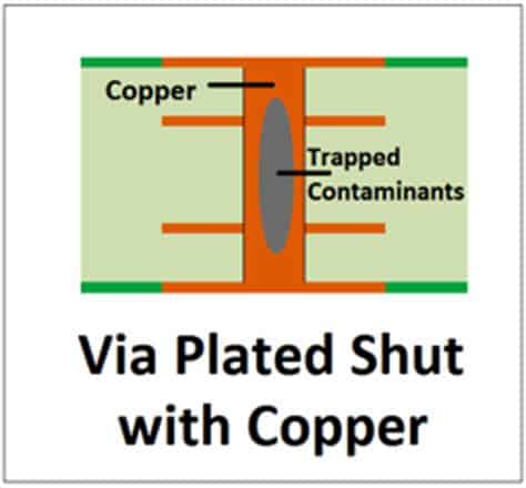
Via size and aspect ratio: As via sizes decrease and aspect ratios increase, it becomes more difficult to achieve consistent and reliable via filling. This is because smaller vias are more prone to issues such as voids, incomplete filling, and poor adhesion.
-
Material selection: The choice of fill material can significantly impact the performance and reliability of the PCB. Factors such as conductivity, thermal stability, and compatibility with the PCB substrate must be carefully considered when selecting a fill material.
-
Process control: Achieving consistent and reliable via filling requires strict control over various process parameters, such as temperature, pressure, and flow rate. Any deviations from the optimal process window can lead to defects and reduced reliability.
-
Cost considerations: Via filling can be a significant cost driver in PCB manufacturing, especially for high-density designs with a large number of vias. Balancing cost with performance and reliability is a key challenge for PCB manufacturers.

Future Trends and Developments in Via Filling Technology
As the demand for high-performance, compact electronic devices continues to grow, via filling technology is expected to evolve to meet these challenges. Some of the future trends and developments in via filling include:
-
Advanced fill materials: Researchers are actively developing new fill materials with improved conductivity, thermal stability, and processing characteristics. These materials may include novel metal alloys, conductive polymers, and nanomaterials.
-
3D printing: The emergence of 3D printing technology in the PCB industry may enable new approaches to via filling, such as the direct printing of conductive materials into the vias.
-
Automation and process optimization: As PCB manufacturing becomes increasingly automated, there will be a growing focus on optimizing via filling processes through the use of advanced process control systems, in-line monitoring, and data analytics.
-
High-density interconnect (HDI) technology: The trend towards HDI PCBs, which feature smaller vias and higher aspect ratios, will drive the development of advanced via filling techniques that can reliably fill these challenging structures.
Frequently Asked Questions (FAQ)
- What is the purpose of via filling in PCB manufacturing?
-
Via filling is used to create electrical connections between different layers of a multi-layer PCB, ensuring reliable electrical conductivity and signal integrity.
-
What materials are commonly used for via filling?
-
Common via fill materials include copper paste, conductive inks, electroplated copper, and conductive epoxies.
-
What are the key challenges in via filling?
-
Some of the key challenges in via filling include achieving consistent and reliable filling of small vias with high aspect ratios, selecting appropriate fill materials, and controlling process parameters to minimize defects.
-
How does via filling impact the performance of a PCB?
-
Via filling can improve the electrical conductivity, signal integrity, and thermal management of a PCB, while also reducing electromagnetic interference and increasing mechanical strength.
-
What are some of the future trends in via filling technology?
- Future trends in via filling include the development of advanced fill materials, the adoption of 3D printing technology, increased automation and process optimization, and the growing importance of high-density interconnect (HDI) technology.
Conclusion
Via filling is a critical process in the manufacturing of high-performance, reliable multi-layer PCBs. By creating electrical connections between layers, via filling ensures proper signal integrity, reduces electromagnetic interference, and enhances the overall performance of the PCB. As electronic devices continue to become smaller, more complex, and more powerful, the importance of via filling will only continue to grow.
While via filling presents several challenges, such as achieving consistent and reliable filling of small, high-aspect-ratio vias, the industry is actively developing new materials, processes, and technologies to address these challenges. From advanced fill materials and 3D printing to automation and process optimization, the future of via filling looks bright, with many exciting developments on the horizon.
As PCB designers and manufacturers continue to push the boundaries of what is possible in electronIC Packaging, via filling will remain a key enabler of innovation and progress in the industry.
No responses yet