What is a 6 Layer PCB Stackup?
A 6 layer PCB stackup refers to the arrangement and order of copper and insulating layers in a 6 layer printed circuit board. The stackup defines the thickness of the PCB and the spacing between copper layers, which impacts the electrical properties, signal integrity, and manufacturability of the board.
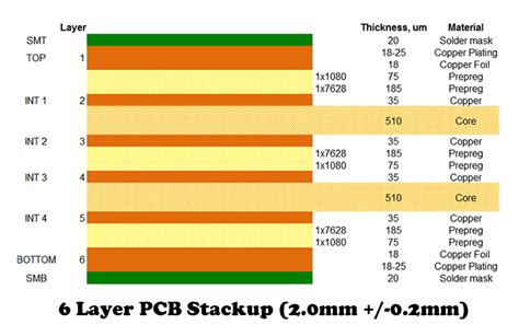
A typical 6 layer PCB will have the following stackup:
| Layer | Material |
|---|---|
| Top Copper | 1 oz copper |
| Prepreg | FR4 |
| Inner Layer 1 | 0.5 oz copper |
| Core | FR4 |
| Inner Layer 2 | 0.5 oz copper |
| Prepreg | FR4 |
| Inner Layer 3 | 0.5 oz copper |
| Core | FR4 |
| Inner Layer 4 | 0.5 oz copper |
| Prepreg | FR4 |
| Bottom Copper | 1 oz copper |
The top and bottom copper layers are typically thicker (1 oz) for durability and current carrying capacity. The inner layers are usually thinner (0.5 oz) to minimize thickness. FR4 glass-reinforced epoxy laminate is the most common PCB core and prepreg material.
Advantages of 6 Layer PCBs
There are several benefits to using a 6 layer PCB:
Increased Routing Density
Having 6 copper layers provides significantly more routing area compared to 2 or 4 layer boards. This allows for higher component density and smaller board sizes.
Better Signal Integrity
The additional ground and power planes in a 6 layer stackup help maintain signal integrity by providing shielding, reducing crosstalk, and controlling impedances. Sensitive signals can be routed between dedicated planes.
Improved Power Delivery
Multiple power planes can be used to efficiently distribute power across the board with low impedance. The inner layers can be used for power planes close to the supply pins of ICs.
Enhanced Thermal Management
Copper planes conduct heat better than FR4. Having more copper layers helps spread and dissipate heat from hot components. Thermal vias can also be used to provide heat sinking to inner planes.
6 Layer PCB Stackup Design Considerations
Designing an optimal 6 layer stackup requires careful planning and execution. Here are some of the key considerations:
Signal Routing
Partition high-speed and low-speed signals onto different layers. Route high-speed traces on outer layers close to ground planes. Provide ground shielding between adjacent signal layers. Avoid crossing split planes with signals.
Power Distribution
Assign dedicated power planes for each supply voltage. Use large area fills for low impedance. Place power planes close to the power pins of ICs. Decouple ICs with capacitors placed near power pins. Use enough vias for low inductance connection to planes.
Grounding
Provide ground planes adjacent to signal layers for shielding and Controlled Impedance. Tie all ground planes together with enough ground vias. Partition analog and digital grounds, tied at a single point. Avoid slots or cuts in ground planes.
Drill Pairs and Vias
Minimize the use of through-hole vias which block routing channels on all layers. Use blind and buried vias where possible to connect only the layers needed. Microvias can be used for high density boards. Stagger vias to avoid split drilling.
Differential Pairs
Route differential pairs on the same layer, tightly coupled, with ground shielding. Match lengths within pairs to maintain phase. Avoid using vias or layer transitions which can cause impedance discontinuities.
Controlled Impedance
Calculate trace widths for controlled impedance based on the stackup geometry and materials. Consult with your manufacturer on their capabilities. Specify controlled impedance requirements on the fab drawing.

6 Layer PCB Stackup Materials
The materials used in a 6 layer PCB stackup play a crucial role in determining its performance and reliability.
Copper Foil
Copper foil is available in different weights, typically measured in ounces per square foot (oz). 1 oz copper (35 μm thick) is commonly used for outer layers, while 0.5 oz (17.5 μm) is used for inner layers to save space and weight. The grade of copper (electrodeposited or rolled annealed) affects its elongation and ability to withstand thermal stress.
Core Laminate
The core laminate is the rigid base material that provides mechanical support for the PCB. FR-4 glass-reinforced epoxy is the most common choice for its good mechanical and electrical properties. Other specialized materials like Rogers or Isola can be used for high-frequency RF applications. The core thickness and glass style influence the rigidity and thermal expansion of the board.
Prepreg
Prepreg (pre-impregnated) is the bonding material used to laminate the core and foil layers together under heat and pressure. It is made of a glass fabric pre-impregnated with a semi-cured epoxy resin. The resin melts and flows during lamination to fill gaps and create a strong bond. The prepreg thickness and resin content determine the spacing between layers and the overall thickness of the board.
Solder Mask
Solder mask is a thin polymer coating applied over the outer copper layers, leaving only the pads and vias exposed. It protects the copper from oxidation, prevents Solder Bridging, and provides electrical insulation. Solder mask is typically green, but other colors are available. Liquid photoimageable (LPI) solder masks offer higher resolution and finer pitch compared to dry film.
Silkscreen
Silkscreen is the white text and graphics printed on top of the solder mask for component labels, logos, and assembly instructions. It is applied using a screen printing process with epoxy ink. The silkscreen should be kept away from pads and openings to avoid interfering with soldering.
6 Layer PCB Stackup Manufacturing Process
The manufacturing process for a 6 layer PCB involves several steps:
-
Inner layer etching: The inner layer copper foils are laminated onto the core substrates and then patterned and etched using photolithography and chemical etching.
-
Layup and lamination: The etched inner layers, prepregs, and outer foils are stacked up in the proper order and alignment. The stackup is then laminated under heat and pressure in a hydraulic press to cure the prepreg and bond the layers together.
-
Drilling: After lamination, holes are drilled through the board for vias and component leads. Computer numerical control (CNC) drilling machines are used for high precision and speed.
-
Plating: The drilled holes are then plated with copper to create electrical connections between layers. Additional copper is plated onto the outer layers to the desired thickness.
-
Outer layer etching: The outer layers are then patterned and etched using photolithography and chemical etching, similar to the inner layers.
-
Solder mask and silkscreen: The solder mask is applied and patterned using photoimaging, and then cured. The silkscreen is then printed onto the solder mask.
-
Surface finish: A surface finish, such as HASL, lead-free HASL, ENIG, or OSP, is applied to the exposed copper to protect it from oxidation and enhance solderability.
-
Electrical test: The finished board is electrically tested using Flying Probe or bed-of-nails testers to check for opens, shorts, and other defects.
Common 6 Layer PCB Stackup Configurations
There are several common 6 layer PCB stackup configurations, each with its own advantages and trade-offs. Here are a few examples:
Signal-Ground
This stackup alternates signal and ground layers for maximum shielding and controlled impedance. It is well-suited for high-speed digital designs.
| Layer | Material |
|---|---|
| Top | Signal |
| Ground | Plane |
| Inner 1 | Signal |
| Power | Plane |
| Inner 2 | Signal |
| Bottom | Signal |
Power-Ground
This stackup dedicates entire layers for power and ground planes, providing low impedance and good isolation. It is useful for mixed-signal designs with sensitive analog circuits.
| Layer | Material |
|---|---|
| Top | Signal |
| Inner 1 | Signal |
| Ground | Plane |
| Power | Plane |
| Inner 2 | Signal |
| Bottom | Signal |
Dual Power
This stackup features two power planes for multiple voltage supplies. It is suitable for complex designs with several power domains.
| Layer | Material |
|---|---|
| Top | Signal |
| Power 1 | Plane |
| Inner 1 | Signal |
| Ground | Plane |
| Inner 2 | Signal |
| Power 2 | Plane |
| Bottom | Signal |
6 Layer PCB Stackup Design Software
Designing a 6 layer PCB stackup requires specialized software tools for creating, simulating, and documenting the stackup. Here are some popular options:
Altium Designer
Altium Designer is a powerful PCB Design platform that includes a stackup manager for defining and visualizing the layer stackup. It can import stackup templates from manufacturers and simulate the impedance and coupling of traces.
Cadence Allegro
Cadence Allegro is another leading PCB design software that offers a stackup editor for creating and managing layer stackups. It can calculate impedances and generate 3D models of the stackup.
Polar Instruments Speedstack
Polar Instruments Speedstack is a dedicated stackup design and documentation tool that integrates with PCB design software. It can optimize stackups for impedance and manufacturability, and generate detailed stackup drawings and reports.
Frequently Asked Questions
What is the typical thickness of a 6 layer PCB?
A typical 6 layer PCB thickness ranges from 0.8 mm to 1.6 mm (31 mil to 63 mil), depending on the thickness of the cores, prepregs, and copper layers used. Thinner boards are more challenging to manufacture and may require specialized materials and processes.
Can you use different materials for the core and prepreg in a 6 layer stackup?
Yes, it is possible to use different materials for the core and prepreg layers in a 6 layer stackup, such as a mix of FR-4 and high-frequency laminates. This can provide the benefits of each material where needed, but may increase the cost and complexity of the board.
How do you choose the right 6 layer stackup for your design?
Choosing the right 6 layer stackup depends on several factors, such as the signal speed, power requirements, component density, and cost targets of your design. Consider simulating and comparing different stackup options to find the best balance of performance and manufacturability.
What are the challenges of designing a 6 layer PCB stackup?
Some of the challenges of designing a 6 layer PCB stackup include maintaining signal integrity, controlling impedances, minimizing crosstalk and EMI, ensuring adequate power delivery, and managing the increased complexity and cost compared to fewer layers. It requires careful planning, simulation, and collaboration with the manufacturer.
How much does a 6 layer PCB cost compared to 4 layers?
The cost of a 6 layer PCB is typically 20-50% higher than a comparable 4 layer board, due to the additional materials, processing steps, and testing required. However, the cost per unit area may be lower for 6 layers due to the increased routing density and smaller board size possible.
Conclusion
In conclusion, a 6 layer PCB stackup offers several advantages over fewer layers, such as increased routing density, better signal integrity, and improved power delivery and thermal management. However, it also requires careful design considerations and trade-offs in terms of materials, manufacturing processes, and cost.
By understanding the principles and best practices of 6 layer stackup design, and using the right tools and collaborating with experienced manufacturers, you can unlock the full potential of this powerful technology for your PCB projects.
No responses yet