Introduction to PCB Design
Printed Circuit Board (PCB) design is a critical aspect of electronics manufacturing. A well-designed PCB ensures reliable performance, reduces manufacturing costs, and minimizes the risk of failures. In this article, we’ll explore essential tips and tricks for designing high-quality PCBs.
Understanding the Basics of PCB Design
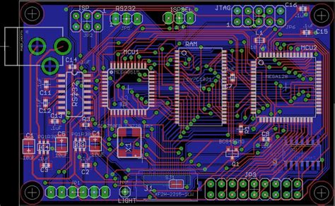
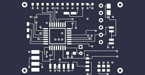
Before diving into specific tips, it’s crucial to understand the fundamentals of PCB design. A PCB consists of several layers of conductive and insulating materials, with components mounted on the surface or embedded within the layers. The primary goal of PCB design is to create a layout that ensures proper electrical connectivity, signal integrity, and mechanical stability.
Key Elements of PCB Design
- Schematic Design: The first step in PCB design is creating a schematic that represents the electrical connections between components.
- Component Placement: Placing components on the PCB layout in a way that minimizes signal interference, reduces trace lengths, and improves manufacturability.
- Routing: Connecting components using conductive traces while adhering to design rules and constraints.
- Manufacturing Considerations: Ensuring the PCB design is compatible with the chosen manufacturing process and meets industry standards.
Tips for Effective Component Placement
Grouping Related Components
Group related components together to minimize trace lengths and improve signal integrity. For example, place decoupling capacitors close to their associated ICs.
Minimizing Crosstalk
Crosstalk occurs when signals from one trace interfere with adjacent traces. To minimize crosstalk:
- Increase the spacing between sensitive traces
- Route critical traces on different layers
- Use guard traces or ground planes to isolate sensitive signals
Thermal Considerations
Consider the thermal characteristics of components when placing them on the PCB. High-power components should be placed away from temperature-sensitive devices and provide adequate heat dissipation.

Routing Best Practices
Choosing the Right Trace Width
The trace width depends on the current carrying capacity and the desired impedance. Use the following table as a general guideline:
| Current (A) | Trace Width (mm) |
|---|---|
| 0.5 | 0.2 |
| 1.0 | 0.4 |
| 2.0 | 0.8 |
| 3.0 | 1.2 |
Minimizing Trace Lengths
Shorter traces reduce signal delays, minimize noise pickup, and improve overall signal integrity. When routing, take the most direct path between components while avoiding obstacles.
Avoiding Right-Angle Traces
Right-angle traces can cause signal reflections and EMI issues. Instead, use 45-degree angles or curved traces to change direction.
Power Distribution Network (PDN) Design
Designing a Robust Power Plane
A well-designed power plane ensures a stable and noise-free power supply to all components. Consider the following tips:
- Use a continuous ground plane to provide a low-impedance return path for signals.
- Provide separate power planes for analog and digital circuits to minimize noise coupling.
- Use power polygons instead of thin traces to distribute power efficiently.
Decoupling Capacitors
Decoupling capacitors help stabilize the power supply and reduce high-frequency noise. Place decoupling capacitors as close as possible to the power pins of ICs.
Signal Integrity Considerations
Controlled Impedance Routing
Controlled impedance routing is essential for high-speed designs to maintain signal integrity. Use the following table to select the appropriate trace width and spacing for common impedance values:
| Impedance (Ω) | Trace Width (mm) | Trace Spacing (mm) |
|---|---|---|
| 50 | 0.2 | 0.2 |
| 75 | 0.15 | 0.3 |
| 100 | 0.1 | 0.4 |
Termination Techniques
Proper termination techniques help prevent signal reflections and ensure clean signal transitions. Common termination techniques include:
- Series termination
- Parallel termination
- RC termination
Choose the appropriate termination technique based on the signal characteristics and the design requirements.
Electromagnetic Compatibility (EMC)
Minimizing Electromagnetic Interference (EMI)
EMI can cause signal integrity issues and violate regulatory requirements. To minimize EMI:
- Keep high-frequency traces short and away from the board edges.
- Use ground planes to shield sensitive signals.
- Implement proper grounding and shielding techniques.
Designing for Electrostatic Discharge (ESD) Protection
ESD can damage sensitive components and cause reliability issues. Incorporate ESD Protection measures such as:
- Using ESD protection diodes on input/output pins
- Providing proper grounding for operators and equipment
- Implementing ESD-safe packaging and handling procedures
Manufacturing Considerations
Design for Manufacturability (DFM)
DFM ensures that the PCB design is compatible with the manufacturing process and reduces the risk of defects. Consider the following DFM Guidelines:
- Adhere to the minimum trace width and spacing specified by the manufacturer.
- Provide adequate clearance between components and traces.
- Use standard component sizes and packages whenever possible.
Panelization
Panelization is the process of grouping multiple PCBs into a single panel for efficient manufacturing. When panelizing PCBs, consider:
- Providing sufficient spacing between individual boards
- Adding Fiducial markers for accurate alignment
- Including tooling holes for handling and registration
FAQ
Q1. What is the difference between a schematic and a PCB layout?
A1. A schematic represents the electrical connections between components using symbols and lines, while a PCB layout shows the physical placement of components and traces on the actual board.
Q2. How do I choose the right PCB material for my design?
A2. The choice of PCB material depends on factors such as the operating frequency, environmental conditions, and cost. Common PCB materials include FR-4, Rogers, and Polyimide. Consult with your PCB manufacturer to select the most suitable material for your application.
Q3. What is the purpose of a ground plane in a PCB?
A3. A ground plane serves as a low-impedance return path for signals, helps reduce EMI, and provides shielding for sensitive signals. It also helps distribute heat evenly across the PCB.
Q4. How can I minimize the impact of vias on signal integrity?
A4. To minimize the impact of vias, use the smallest possible via size, place vias away from critical signals, and avoid unnecessary layer changes. In high-speed designs, consider using blind or buried vias to reduce the via stub effect.
Q5. What are some common PCB design software tools?
A5. Some popular PCB design software tools include:
- Altium Designer
- Cadence OrCAD
- KiCad
- Eagle
- Mentor Graphics PADS
Each tool has its own strengths and weaknesses, so choose the one that best suits your design requirements and budget.
Conclusion
Designing a high-quality PCB requires careful consideration of various factors, including component placement, routing, signal integrity, power distribution, and manufacturing considerations. By following the tips and best practices outlined in this article, you can create PCBs that are reliable, manufacturable, and meet the desired performance requirements. Remember to consult with your PCB manufacturer early in the design process to ensure compatibility and optimize your design for manufacturing.
No responses yet