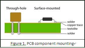
Why is PCB component clearance Important?
Proper component clearance on a PCB is essential for several reasons:
-
Manufacturing feasibility: Sufficient clearance between components allows for easier assembly and soldering processes, reducing the risk of manufacturing defects.
-
Electrical integrity: Adequate spacing between components prevents short circuits, signal interference, and other electrical issues that can compromise the functionality of the PCB.
-
Heat dissipation: Proper clearance facilitates better airflow and heat dissipation, preventing components from overheating and failing prematurely.
-
Mechanical stability: Appropriate spacing between components reduces the risk of physical damage during handling, vibration, or shock.
IPC Standards for PCB Component Clearance
The IPC has established several standards that address PCB component clearance requirements. The most relevant standards are:
IPC-2221: Generic Standard on Printed Board Design
IPC-2221 is a comprehensive standard that provides guidelines for the design of printed circuit boards. It covers various aspects of PCB Design, including component clearances. Some key points from IPC-2221 regarding component clearance include:
- Minimum clearance between component bodies: 0.25 mm (0.010 in)
- Minimum clearance between component leads/terminals: 0.20 mm (0.008 in)
- Minimum clearance between component bodies and board edges: 0.50 mm (0.020 in)
IPC-7351: Generic Requirements for Surface Mount Design and Land Pattern Standard
IPC-7351 focuses on surface mount technology (SMT) and provides guidelines for Land Pattern Design and component placement. This standard defines three levels of density for SMT component placement:
- Level A (Least Dense): Minimum clearance of 0.50 mm (0.020 in) between components
- Level B (Moderately Dense): Minimum clearance of 0.25 mm (0.010 in) between components
- Level C (Most Dense): Minimum clearance of 0.13 mm (0.005 in) between components
The following table summarizes the minimum component clearances for each density level:
| Density Level | Minimum Component Clearance |
|---|---|
| Level A | 0.50 mm (0.020 in) |
| Level B | 0.25 mm (0.010 in) |
| Level C | 0.13 mm (0.005 in) |
IPC-7093: Design and Assembly Process Implementation for Bottom Termination Components
IPC-7093 provides guidance for designing and assembling PCBs with bottom termination components (BTCs), such as ball grid arrays (BGAs) and quad flat no-leads (QFNs). This standard recommends the following minimum clearances for BTCs:
- Minimum clearance between BTC and adjacent components: 0.50 mm (0.020 in)
- Minimum clearance between BTC and board edge: 0.50 mm (0.020 in)
Best Practices for Designing PCBs with Appropriate Component Clearance
To ensure optimal PCB Performance and manufacturability, designers should follow these best practices when considering component clearance:
-
Adhere to IPC standards: Always refer to the relevant IPC standards for guidance on minimum component clearances based on the specific design requirements and manufacturing capabilities.
-
Consider component size and packaging: Larger components or those with unique packaging may require additional clearance to accommodate their dimensions and assembly needs.
-
Account for thermal considerations: Components that generate significant heat should be spaced farther apart to allow for adequate heat dissipation and to prevent thermal stress on nearby components.
-
Plan for assembly and inspection: Provide sufficient clearance for assembly equipment, such as pick-and-place machines and soldering tools, as well as for inspection and testing processes.
-
Collaborate with manufacturers: Consult with your PCB Manufacturer early in the design process to discuss their specific clearance requirements and capabilities, ensuring a smooth transition from design to production.

Frequently Asked Questions
-
What happens if PCB component clearances are too small?
If component clearances are too small, it can lead to manufacturing difficulties, such as bridging during soldering, short circuits, and component damage. It can also hinder proper heat dissipation and increase the risk of electrical interference. -
Can I use smaller component clearances than those recommended by IPC?
While it is possible to use smaller clearances, it is not advisable unless you have thoroughly consulted with your PCB manufacturer and have confirmed their ability to reliably produce boards with reduced clearances. Deviating from IPC standards may increase the risk of manufacturing defects and compromise the performance and reliability of the PCB. -
Do component clearances affect PCB signal integrity?
Yes, component clearances can impact signal integrity. Insufficient clearance between components can lead to signal coupling, crosstalk, and electromagnetic interference (EMI), which can degrade the quality of signals transmitted through the PCB. -
How do I determine the appropriate component clearance for my PCB design?
To determine the appropriate component clearance, start by referring to the relevant IPC standards based on your design requirements and the types of components used. Consider factors such as component size, thermal characteristics, and assembly processes. Consult with your PCB manufacturer to discuss their specific clearance capabilities and recommendations. -
Are there any tools available to help with component clearance design?
Yes, many PCB design software packages include tools and features that assist with component placement and clearance checking. These tools can automatically detect clearance violations and provide visual feedback to help designers optimize component spacing. Additionally, some software offers built-in libraries with component footprints that adhere to IPC standards, simplifying the design process.
Conclusion
PCB component clearance is a critical aspect of printed circuit board design that directly impacts manufacturing feasibility, electrical performance, thermal management, and mechanical stability. By adhering to IPC standards and following best practices for component spacing, designers can create PCBs that are reliable, manufacturable, and meet the required functionality. Always collaborate with your PCB manufacturer to ensure that your design aligns with their capabilities and recommendations, and utilize PCB design software tools to streamline the component placement and clearance checking process. By prioritizing appropriate component clearance, you can minimize the risk of design and manufacturing issues, ultimately leading to a successful and robust PCB product.

No responses yet