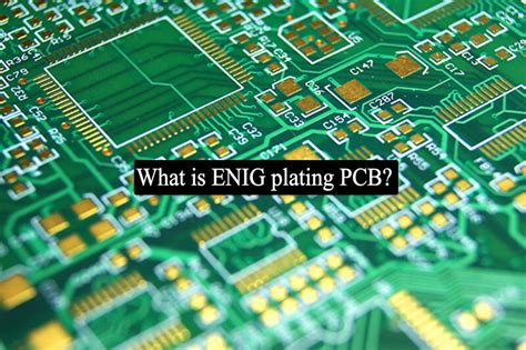
Introduction to ENIG (Electroless Nickel Immersion Gold)
ENIG, which stands for Electroless Nickel Immersion Gold, is a popular surface finish used in the manufacturing of printed circuit boards (PCBs). Also known as Che Ni/Au, this finish combines the benefits of electroless nickel plating and immersion gold plating to create a reliable and cost-effective surface that enhances the solderability, durability, and shelf life of PCBs.
What is a PCB Surface Finish?
A PCB surface finish is a coating applied to the exposed copper surfaces of a printed circuit board to protect the copper from oxidation and corrosion, while also providing a solderable surface for component assembly. The choice of surface finish can significantly impact the performance, reliability, and manufacturability of the final product.
Why Choose ENIG?
ENIG has gained widespread acceptance in the electronics industry due to its numerous advantages over other surface finishes. Some of the key benefits of ENIG include:
- Excellent solderability
- Long shelf life
- Good corrosion resistance
- Compatibility with a wide range of components and assembly processes
- Suitable for high-frequency and high-speed applications
- Relatively low cost compared to other premium surface finishes
The ENIG Process
The ENIG process involves several steps to create the desired surface finish on the PCB. Let’s take a closer look at each step:
Step 1: Cleaning and Preparation
Before applying the ENIG finish, the PCB undergoes a thorough cleaning process to remove any contaminants, such as dirt, grease, or oxidation, from the copper surface. This step ensures proper adhesion of the subsequent layers and prevents any defects in the final finish.
Step 2: Electroless Nickel Plating
Once the PCB is clean, it is immersed in an electroless nickel plating bath. This bath contains a nickel salt solution and a reducing agent, which work together to deposit a thin, uniform layer of nickel onto the copper surface without the use of an external electrical current. The nickel layer typically ranges from 3 to 6 microns in thickness and serves as a barrier between the copper and the immersion gold layer.
The electroless nickel plating process offers several advantages:
- Uniform coverage, even on complex geometries and through-holes
- Good corrosion resistance
- Excellent adhesion to the copper substrate
- Provides a smooth, solderable surface for the immersion gold layer
Step 3: Immersion Gold Plating
After the electroless nickel plating, the PCB is rinsed and then immersed in an immersion gold plating bath. This bath contains a gold salt solution that deposits a thin layer of gold, typically 0.05 to 0.2 microns thick, onto the nickel surface through a chemical displacement reaction.
The immersion gold layer serves several purposes:
- Protects the nickel layer from oxidation and corrosion
- Enhances the solderability of the surface
- Provides a clean, conductive surface for component assembly
- Improves the shelf life of the PCB
Step 4: Rinsing and Drying
After the immersion gold plating, the PCB is thoroughly rinsed to remove any residual plating chemicals and then dried using hot air or an oven. The resulting ENIG surface finish is now ready for component assembly or storage.

Advantages of ENIG
ENIG offers numerous benefits that make it a popular choice for a wide range of PCB Applications. Let’s explore some of these advantages in more detail:
Excellent Solderability
One of the primary reasons for choosing ENIG is its excellent solderability. The thin, pure gold layer provides a clean, oxide-free surface that promotes strong and reliable solder joints. This is particularly important for fine-pitch components and high-density PCB Designs, where solderability is critical for ensuring proper electrical connections.
Long Shelf Life
ENIG-finished PCBs have a long shelf life, typically up to 12 months or more, when stored in proper conditions. The immersion gold layer effectively protects the underlying nickel and copper from oxidation and corrosion, maintaining the solderability of the surface over an extended period. This is particularly beneficial for PCBs that may not be assembled immediately after manufacturing or for those that require long-term storage before use.
Good Corrosion Resistance
The electroless nickel layer in ENIG provides good corrosion resistance, protecting the copper substrate from the effects of harsh environmental conditions. This is particularly important for PCBs that may be exposed to moisture, humidity, or other corrosive agents during their service life. The immersion gold layer further enhances the corrosion resistance by preventing oxidation of the nickel surface.
Compatibility with Various Components and Assembly Processes
ENIG is compatible with a wide range of components and assembly processes, making it a versatile surface finish option. It can be used with both through-hole and surface-mount components, and is suitable for various soldering methods, including Wave Soldering, reflow soldering, and hand soldering. Additionally, ENIG is compatible with advanced packaging technologies, such as ball grid arrays (BGAs) and chip-scale packages (CSPs).
Suitable for High-Frequency and High-Speed Applications
ENIG is an excellent choice for high-frequency and high-speed PCB applications, such as those found in telecommunications, automotive, and aerospace industries. The thin, uniform layers of nickel and gold provide a smooth, conductive surface that minimizes signal loss and maintains signal integrity. This is particularly important for high-speed digital circuits and RF applications, where signal quality is critical for proper functioning.
Cost-Effectiveness
While ENIG is considered a premium surface finish, it is still relatively cost-effective compared to other high-end options, such as gold plating or palladium. The electroless nickel and immersion gold processes are well-established and can be easily integrated into existing PCB manufacturing lines, reducing the overall cost of implementation. Additionally, the long shelf life and excellent solderability of ENIG can help reduce rework and scrap costs associated with poor solder joints or oxidized surfaces.

Disadvantages of ENIG
Despite its many advantages, ENIG does have some limitations and potential drawbacks that should be considered when selecting a surface finish for a particular application. Some of these disadvantages include:
Black Pad Syndrome
One of the most well-known issues associated with ENIG is the occurrence of “black pad syndrome.” This phenomenon is characterized by the formation of a thin, brittle layer of nickel-phosphorus between the electroless nickel and immersion gold layers. This brittle layer can lead to weak or non-wetting solder joints, which can cause reliability issues in the final assembly.
Black pad syndrome is typically caused by improper process control during the ENIG plating process, such as excessive immersion time in the gold bath or contamination of the plating solutions. Proper process control and regular monitoring can help minimize the risk of black pad formation.
Higher Cost Compared to Other Surface Finishes
While ENIG is cost-effective compared to other premium surface finishes, it is still more expensive than basic options, such as hot air solder leveling (HASL) or organic solderability preservatives (OSP). The higher cost is due to the additional processing steps and the use of gold in the immersion plating process. However, the benefits of ENIG, such as improved solderability and longer shelf life, can often justify the added cost for many applications.
Potential for Gold Embrittlement
In some cases, the thin immersion gold layer in ENIG can diffuse into the solder joint during the soldering process, leading to gold embrittlement. This can result in brittle, less reliable solder joints that are more susceptible to cracking or failure under mechanical stress or thermal cycling.
The risk of gold embrittlement can be minimized by controlling the thickness of the immersion gold layer and by using solder alloys with a higher melting point, such as lead-free SAC (tin-silver-copper) alloys.

Applications of ENIG
ENIG is widely used in various industries and applications where reliable, solderable, and durable PCB surfaces are required. Some common applications include:
- Consumer electronics
- Automotive electronics
- Telecommunications equipment
- Medical devices
- Aerospace and defense systems
- Industrial control and automation
In these applications, ENIG provides a robust and reliable surface finish that can withstand the demands of harsh environments, high-frequency signals, and fine-pitch component assembly.
Alternatives to ENIG
While ENIG is a popular choice for many PCB applications, there are other surface finish options available that may be more suitable for specific requirements or budgets. Some common alternatives to ENIG include:
HASL (Hot Air Solder Leveling)
HASL is a widely used and cost-effective surface finish that involves applying a layer of molten solder to the PCB surface and then using hot air to remove the excess, leaving a thin, solderable layer. HASL is compatible with most soldering processes and provides good solderability, but it may not be suitable for fine-pitch components or high-density designs due to its relatively uneven surface.
OSP (Organic Solderability Preservatives)
OSP is a simple and low-cost surface finish that involves applying a thin, organic coating to the copper surface to protect it from oxidation. OSP provides good solderability and is suitable for most soldering processes, but it has a limited shelf life and may not provide sufficient protection for harsh environments or long-term storage.
Immersion Silver
Immersion silver is a surface finish that deposits a thin layer of silver onto the copper surface through a chemical displacement reaction. It provides excellent solderability and is a cost-effective alternative to ENIG for some applications. However, immersion silver has a limited shelf life and may be susceptible to tarnishing or oxidation over time.
Immersion Tin
Immersion tin is another surface finish option that involves depositing a thin layer of tin onto the copper surface. It provides good solderability and is relatively low-cost, but it has a limited shelf life and may be prone to tin whisker formation, which can cause short circuits or reliability issues in some applications.
Frequently Asked Questions (FAQ)
-
Q: What does ENIG stand for?
A: ENIG stands for Electroless Nickel Immersion Gold, which refers to the two primary layers that make up this surface finish. -
Q: What are the typical thicknesses of the nickel and gold layers in ENIG?
A: The electroless nickel layer is typically 3 to 6 microns thick, while the immersion gold layer is usually 0.05 to 0.2 microns thick. -
Q: How long can ENIG-finished PCBs be stored before assembly?
A: ENIG-finished PCBs can typically be stored for up to 12 months or more, when kept in proper conditions, without significant degradation of solderability or surface quality. -
Q: What is black pad syndrome, and how can it be prevented?
A: Black pad syndrome is a defect that can occur in ENIG-finished PCBs, characterized by a thin, brittle layer of nickel-phosphorus between the nickel and gold layers. It can be prevented through proper process control and regular monitoring of the plating solutions. -
Q: Is ENIG suitable for high-frequency and high-speed PCB applications?
A: Yes, ENIG is an excellent choice for high-frequency and high-speed applications, as it provides a smooth, conductive surface that minimizes signal loss and maintains signal integrity.
Conclusion
In conclusion, ENIG (Electroless Nickel Immersion Gold) is a highly reliable and cost-effective surface finish for printed circuit boards, offering excellent solderability, long shelf life, and good corrosion resistance. Its compatibility with a wide range of components and assembly processes, along with its suitability for high-frequency and high-speed applications, makes it a popular choice for various industries.
While ENIG has some potential drawbacks, such as the risk of black pad syndrome and higher cost compared to basic surface finishes, these can be mitigated through proper process control and design considerations. Overall, the benefits of ENIG make it a valuable option for PCB manufacturers and designers seeking a high-quality, long-lasting surface finish.
As technology continues to advance and the demand for more robust and reliable PCBs grows, ENIG is likely to remain a preferred choice for many applications. By understanding the advantages, disadvantages, and proper implementation of ENIG, PCB manufacturers can make informed decisions and deliver high-quality products that meet the evolving needs of the electronics industry.
No responses yet