Overview of PCB Layer Stackup
A typical PCB consists of multiple layers laminated together:
| Layer | Description |
|---|---|
| Solder Mask (top) | Insulating layer that protects copper traces |
| Copper Layer (top) | Conductive layer for component connections |
| Core | Rigid insulating material (e.g. FR-4 fiberglass) |
| Copper Layer (bottom) | Conductive layer for component connections |
| Solder Mask (bottom) | Insulating layer that protects copper traces |
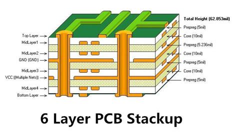
Additional copper layers can be added by laminating more core material and Copper Foil. Two-layer boards have copper on the top and bottom, while 4-layer, 6-layer, 8-layer and higher layer counts alternate copper and insulating core material.
PCB Mechanical Layers
In addition to the electrical copper layers, a PCB design includes mechanical layers that define the physical board shape, drill holes, slots, cutouts, text labels, and other structural features. These mechanical layers are not actual physical layers in the manufactured board, but rather instructions for fabrication.
Board Outline Layer
The board outline layer defines the shape and size of the PCB. It shows where the board will be cut out from the larger manufacturing panel. The board outline is typically a simple rectangular shape, but can include notches, tabs, or complex curved contours as needed to fit the enclosure.
A standard PCB manufacturing panel is 18 x 24 inches (457 x 610 mm). Smaller boards are panelized to fit as many as possible in one panel for efficient fabrication and assembly.
Drill Layers and Drill Table
Drill layers specify the location and size of holes that pass through the PCB. These include:
- Plated through holes for mounting components
- Vias for connecting traces on different layers
- Unplated mounting holes for screws, standoffs, etc.
The drill table lists the diameter and plating requirements for each drill hit. Standard drill sizes range from 0.2 mm to 6.35 mm. Smaller holes cost more to fabricate.
Mill Layer
The mill layer (also called route layer) defines an internal cutout or slot in the board. This could be a large opening to fit another component, a long narrow slot for a connector, or a cavity to recess a component below the board surface.
Milled features are routed out using a CNC milling machine after the board layers are laminated together. The mill layer shows the path the milling tool will follow.
Silkscreen Layers
Silkscreen layers add text labels and visual indicators to help with PCB Assembly and troubleshooting. The top and bottom silkscreen are printed onto the outer solder mask layers.
Typical silkscreen markings include:
- Component outlines and reference designators
- Test points
- Company name and logo
- Board name and revision number
- Certifications and regulatory symbols
- Pin 1 indicators and polarity marks
The silkscreen layers are called out separately from the solder mask in the design files. White epoxy ink is most common, but other colors are available.
Solder Paste Layers
Solder paste layers show where solder paste will be applied to the board prior to placing components. The paste layer artwork is used to make a metal stencil for applying the paste.
Openings in the solder paste layer align with component pads on the top and/or bottom copper layers. The size of the openings determines how much solder is deposited.
Assembly Drawing Layers
Assembly drawing layers provide additional information for assembling, testing, and servicing the completed PCB. These could include:
- Component heights
- 3D views
- Critical tolerances
- Torque specs for screw terminals
- Cable and harness connections
- Testing and troubleshooting procedures
This information can be included on the fabrication drawing, or as a separate document for the contract manufacturer.

Mechanical Layer Considerations
Material Selection
The choice of PCB base material affects both electrical performance and mechanical durability. FR-4 fiberglass epoxy laminate is the most common material for rigid PCBs. It provides good dielectric properties and mechanical strength at reasonable cost.
Specialized materials may be needed for high-frequency circuits, controlled impedance, high-temperature, or flexible applications. The IPC-4101 specifications define standard PCB materials.
Minimum Drill Size and Spacing
Smaller drills and tighter spacing increase PCB fabrication costs. For most designs, the minimum drill size is 0.2-0.25 mm. Microvias can be as small as 0.1 mm but require specialized manufacturing processes.
The minimum spacing between drills is determined by the PCB material and thickness. Thinner materials allow closer spacing. Typical minimums are:
| Drill Size | Minimum Spacing |
|---|---|
| 0.2-0.5 mm | 0.5 mm |
| 0.5-1.0 mm | 0.8 mm |
| 1.0-1.5 mm | 1.0 mm |
| > 1.5 mm | 1.5 mm |
Keepout Areas
Mechanical keepout areas define where components and copper features are not allowed. These could be areas for mounting holes, connector cutouts, or to avoid interference with other parts of the assembly.
The keepout areas are defined on separate drawing layers, not the copper layers themselves. The design software can use keepout layers to check for placement violations.
Panelization
Panelization is the process of laying out multiple identical circuit boards in an array to be fabricated as one panel. This is an efficient way to manufacture small boards.
Panelization can use tab-routing, where small tabs hold the boards in the panel until they are separated by breaking the tabs. Or a V-scoring process can be used to cut part-way through the panel so the boards can be snapped apart after assembly.
The panel design must include fiducial marks for aligning the automated assembly and test equipment. Tooling holes are also needed to hold the panel in place during fabrication.

FAQ
What is the purpose of mechanical layers in PCB design?
Mechanical layers define the physical structure and features of the PCB, including the board outline, drills, slots, silkscreen markings, and assembly information. They provide essential fabrication instructions in addition to the electrical wiring of the copper layers.
How do mechanical layers affect PCB manufacturing cost?
The complexity of the mechanical layers can significantly impact the cost of fabricating a PCB. Smaller drills, tighter spacing, and intricate board outlines require more precise equipment and processing, increasing the cost. Using standard drill sizes, minimizing the number of different drill sizes, and keeping the board shape simple help control fabrication costs.
What is the difference between plated and non-plated drill holes?
Plated drill holes have a conductive metal coating on the inside of the hole to electrically connect copper layers on different sides of the board. These are used for vias and component leads. Non-plated holes are used for mounting the PCB to the chassis or other mechanical functions where electrical connection is not needed.
How do I specify different finishes on mechanical layers?
The PCB fabrication drawing can specify different Surface Finishes on mechanical layers. For example, exposed copper areas may be plated with gold, nickel, or tin to prevent corrosion. The solder mask and silkscreen layers can also use different colors. Discuss the available options with the PCB manufacturer to ensure the design is compatible with their processes.
What is the importance of keepout layers in PCB design?
Keepout layers define areas on the PCB where components and traces are not allowed. This could be for mechanical clearance, such as around mounting holes or connector cutouts. Keepouts can also define safety zones to ensure proper spacing between high-voltage components. By using keepout layers, the PCB Design Software can automatically check for placement violations, ensuring the design is manufacturable and meets safety requirements.

No responses yet