Introduction to PCB Manufacturing
Printed Circuit Board (PCB) manufacturing is a complex process that involves the creation of electronic circuits on a non-conductive substrate. PCBs are essential components in virtually all electronic devices, from smartphones and computers to industrial equipment and aerospace systems. The manufacturing process requires precision, expertise, and advanced technology to ensure the highest quality and reliability of the final product.
The Importance of PCB Manufacturing
PCB manufacturing plays a crucial role in the electronics industry, as it enables the production of compact, efficient, and reliable electronic devices. Some of the key benefits of PCB manufacturing include:
-
Miniaturization: PCBs allow for the integration of multiple electronic components into a small, compact package, enabling the creation of smaller and more portable devices.
-
Reliability: Well-manufactured PCBs ensure stable connections between components, minimizing the risk of failures and malfunctions.
-
Cost-effectiveness: PCB manufacturing allows for the mass production of electronic circuits, reducing costs and increasing efficiency compared to traditional point-to-point wiring.
-
Design flexibility: PCBs can be designed to accommodate a wide range of electronic components and configurations, enabling the creation of custom solutions for specific applications.
The PCB Manufacturing Process
The PCB manufacturing process involves several key steps, each of which requires specialized equipment and expertise. The main stages of PCB manufacturing are:
1. PCB Design
The first step in PCB manufacturing is the design of the electronic circuit. This involves creating a schematic diagram that shows the connections between the various components, as well as a layout that specifies the physical placement of the components on the PCB. PCB design software, such as Altium Designer or Eagle, is used to create these files.
2. PCB Fabrication
Once the design is complete, the PCB fabrication process begins. This involves the following sub-steps:
2.1 Substrate Preparation
The substrate, typically a glass-reinforced epoxy laminate (FR-4), is cut to the required size and shape. Copper foil is then laminated onto the substrate using heat and pressure.
2.2 Drilling
Holes are drilled into the substrate to accommodate through-hole components and to create vias that connect different layers of the PCB.
2.3 Patterning
A photoresist layer is applied to the copper foil and exposed to UV light through a photomask that contains the circuit pattern. The exposed areas of the photoresist are then removed, leaving behind a protective layer in the shape of the circuit.
2.4 Etching
The exposed copper is removed using a chemical etching process, leaving behind the desired circuit pattern.
2.5 Plating
Additional copper is plated onto the remaining copper traces to increase their thickness and improve their current-carrying capacity. A thin layer of tin or gold may also be applied to protect the copper from oxidation and improve solderability.
2.6 Solder Mask Application
A solder mask, typically a green or blue polymer, is applied to the PCB to protect the copper traces from short circuits and to prevent solder from bridging adjacent pads during assembly.
2.7 Silkscreen
A silkscreen layer is applied to the PCB to add text, logos, and component identifiers. This helps with the assembly process and makes the PCB easier to troubleshoot.
3. PCB Assembly
After the PCB fabrication process is complete, the components are assembled onto the board. This can be done manually for low-volume production or prototypes, but is typically automated for high-volume manufacturing. The main steps in PCB assembly are:
3.1 Solder Paste Application
Solder paste, a mixture of tiny solder particles and flux, is applied to the pads on the PCB using a stencil or syringe.
3.2 Component Placement
The electronic components are placed onto the PCB, either manually or using automated pick-and-place machines. Surface mount devices (SMDs) are placed directly onto the pads, while through-hole components are inserted into the drilled holes.
3.3 Soldering
The PCB is heated in a reflow oven, causing the solder paste to melt and form a permanent connection between the components and the PCB pads. For through-hole components, wave soldering or selective soldering techniques may be used.
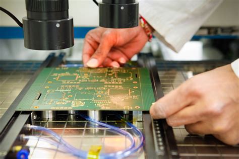
3.4 Inspection and Testing
The assembled PCB undergoes a series of inspections and tests to ensure that all components are properly placed and soldered, and that the board functions as intended. This may include automated optical inspection (AOI), X-ray inspection, and functional testing.
4. Final Finishing and Packaging
Once the PCB has passed all inspections and tests, it may undergo additional finishing processes, such as conformal coating to protect against moisture and contaminants, or potting to provide mechanical support and insulation. The finished PCBs are then packaged and shipped to the customer.

Advanced PCB Manufacturing Techniques
As electronic devices become more complex and demanding, PCB manufacturing technologies have evolved to keep pace. Some of the advanced techniques used in modern PCB manufacturing include:
High Density Interconnect (HDI) PCBs
HDI PCBs feature finer traces, smaller vias, and higher component density than traditional PCBs. This allows for the creation of more compact and powerful electronic devices. HDI PCBs often incorporate microvias, which are tiny holes that connect adjacent layers, and buried or blind vias, which do not extend through the entire thickness of the board.
Flexible and Rigid-flex PCBs
Flexible PCBs are made from thin, flexible substrates that can be bent or folded to fit into tight spaces or conform to curved surfaces. Rigid-flex PCBs combine both rigid and flexible sections, allowing for even greater design flexibility. These types of PCBs are commonly used in wearable electronics, medical devices, and aerospace applications.
Multilayer PCBs
Multilayer PCBs consist of multiple layers of copper traces separated by insulating layers. This allows for more complex circuits and higher component density than single or double-layer boards. Multilayer PCBs can have anywhere from 4 to over 40 layers, depending on the application.
Embedded Components
Embedded components, such as resistors, capacitors, and even active devices like microcontrollers, are placed inside the layers of the PCB rather than on the surface. This can save space, reduce signal interference, and improve reliability.
3D Printed Electronics
3D printing technology is increasingly being used to create PCBs and electronic components. This allows for greater design freedom, faster prototyping, and the ability to create complex, three-dimensional structures that would be difficult or impossible to achieve with traditional manufacturing methods.

PCB Manufacturing Standards and Certifications
To ensure the quality and reliability of PCBs, manufacturers must adhere to various industry standards and certifications. Some of the most important standards and certifications include:
IPC Standards
The Association Connecting Electronics Industries (IPC) publishes a wide range of standards for PCB design, fabrication, and assembly. These include:
- IPC-A-600: Acceptability of Printed Boards
- IPC-6010: Qualification and Performance Specification for High-Density Interconnect (HDI) Layers or Boards
- IPC-7351: Generic Requirements for Surface Mount Design and Land Pattern Standard
UL Certification
Underwriters Laboratories (UL) is a global safety certification company that tests and certifies PCBs and electronic components. UL certification ensures that products meet specific safety and performance requirements.
ISO Certification
The International Organization for Standardization (ISO) publishes standards for quality management systems, environmental management, and other aspects of manufacturing. PCB manufacturers may hold certifications such as ISO 9001 (quality management) or ISO 14001 (environmental management) to demonstrate their commitment to quality and sustainability.

Choosing a PCB Manufacturer
When selecting a PCB manufacturer, it is important to consider several key factors to ensure that you receive high-quality boards that meet your specific requirements. Some of the most important considerations include:
Technical Capabilities
Make sure that the manufacturer has the necessary equipment, expertise, and experience to produce PCBs that meet your technical specifications. This includes factors such as minimum trace width and spacing, hole size, layer count, and material selection.
Quality Control
Choose a manufacturer with a robust quality control system in place, including automated inspections, testing, and documentation. Look for certifications such as IPC and ISO to ensure that the manufacturer adheres to industry standards.
Lead Time and Pricing
Consider the manufacturer’s lead times and pricing structure to ensure that they can meet your delivery and budget requirements. Keep in mind that lower prices may sometimes come at the expense of quality or reliability.
Customer Support and Communication
Select a manufacturer with responsive and knowledgeable customer support, as well as clear communication channels. This can be particularly important if you are working on a complex or custom design that requires close collaboration between your team and the manufacturer.
The Future of PCB Manufacturing
As technology continues to advance, PCB manufacturing is poised to evolve in exciting new directions. Some of the trends and developments that are shaping the future of PCB manufacturing include:
Increased Miniaturization
The demand for smaller, more compact electronic devices is driving the development of ever-smaller PCBs with higher component density. This will require new materials, manufacturing processes, and design tools to enable the creation of ultra-miniaturized circuits.
Sustainable Manufacturing
There is a growing focus on sustainable manufacturing practices in the PCB industry, including the use of eco-friendly materials, renewable energy, and waste reduction strategies. Manufacturers are also exploring ways to improve the recyclability and end-of-life management of PCBs.
Intelligent and Adaptive PCBs
The integration of sensors, microcontrollers, and other active components into PCBs is enabling the creation of intelligent and adaptive systems that can respond to changing conditions or user needs. This could lead to the development of self-healing circuits, energy-harvesting PCBs, and other innovative applications.
Additive Manufacturing
Additive manufacturing techniques, such as 3D printing, are becoming increasingly sophisticated and are expected to play a larger role in PCB manufacturing in the coming years. This could enable the creation of complex, three-dimensional circuit structures and the rapid prototyping of new designs.
Frequently Asked Questions (FAQ)
- What is the difference between a PCB and a PCBA?
-
A PCB (Printed Circuit Board) is the bare board without any components attached. A PCBA (Printed Circuit Board Assembly) is a PCB with all the electronic components soldered onto it, ready for use in an electronic device.
-
What are the most common materials used in PCB substrates?
-
The most common PCB substrate material is FR-4, a glass-reinforced epoxy laminate. Other materials include polyimide for flexible PCBs, aluminum for metal-core PCBs, and ceramic for high-temperature applications.
-
What is the difference between surface mount (SMT) and through-hole (THT) components?
-
Surface mount components are mounted directly onto the pads on the surface of the PCB, while through-hole components have leads that are inserted into holes drilled through the board. SMT components are generally smaller and better suited for automated assembly, while THT components are often used for larger or higher-power components.
-
How long does it typically take to manufacture a PCB?
-
The lead time for PCB manufacturing can vary depending on the complexity of the design, the manufacturing process, and the manufacturer’s workload. Typical lead times range from a few days for simple, quick-turn PCBs to several weeks for complex, high-layer-count boards.
-
What is the minimum feature size that can be achieved in PCB manufacturing?
- The minimum feature size depends on the capabilities of the specific manufacturer and the chosen manufacturing process. For standard PCB fabrication, minimum trace widths and spaces of around 0.1 mm (4 mil) are common. Advanced HDI processes can achieve feature sizes down to 0.05 mm (2 mil) or smaller.
Conclusion
PCB manufacturing is a complex and constantly evolving field that plays a critical role in the production of modern electronic devices. By understanding the key steps in the manufacturing process, as well as the advanced techniques, standards, and certifications involved, designers and engineers can make informed decisions when selecting a PCB manufacturer and ensuring the quality and reliability of their products.
As technology continues to advance, PCB manufacturing will face new challenges and opportunities, from increasing miniaturization and sustainability to the integration of intelligent and adaptive features. By staying at the forefront of these developments, PCB manufacturers can help drive innovation and enable the creation of the next generation of electronic devices.
| PCB Manufacturing Process | Description |
|---|---|
| PCB Design | Creating the schematic diagram and layout of the electronic circuit |
| PCB Fabrication | Manufacturing the bare PCB, including substrate preparation, drilling, patterning, etching, plating, solder mask application, and silkscreening |
| PCB Assembly | Attaching the electronic components to the PCB, including solder paste application, component placement, soldering, and inspection |
| Final Finishing and Packaging | Additional processes such as conformal coating or potting, followed by packaging and shipping |
| Advanced PCB Manufacturing Techniques | Description |
|---|---|
| High Density Interconnect (HDI) PCBs | PCBs with finer traces, smaller vias, and higher component density |
| Flexible and Rigid-Flex PCBs | PCBs made from flexible substrates or combining rigid and flexible sections |
| Multilayer PCBs | PCBs with multiple layers of copper traces separated by insulating layers |
| Embedded Components | Components placed inside the layers of the PCB rather than on the surface |
| 3D Printed Electronics | Using 3D printing technology to create PCBs and electronic components |
No responses yet