Introduction to PCB Ultraviolet Lasers
Printed Circuit Boards (PCBs) are the backbone of modern electronics, found in everything from smartphones to aerospace systems. The manufacturing process of PCBs has evolved significantly over the years, with the introduction of advanced technologies like ultraviolet (UV) lasers. PCB ultraviolet lasers have revolutionized the way PCBs are fabricated, offering higher precision, faster processing speeds, and improved reliability compared to traditional methods.
What are PCB Ultraviolet Lasers?
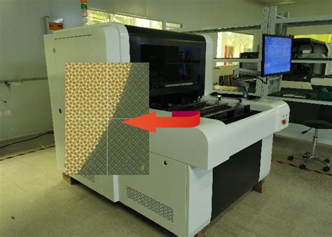
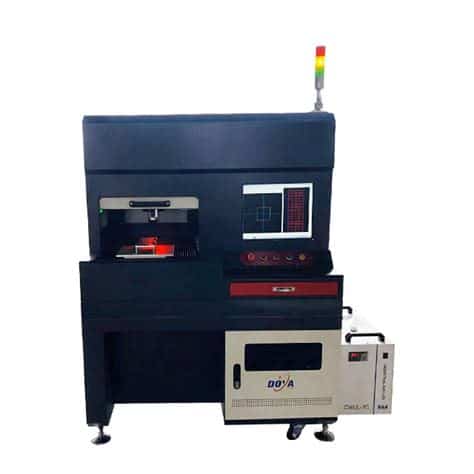
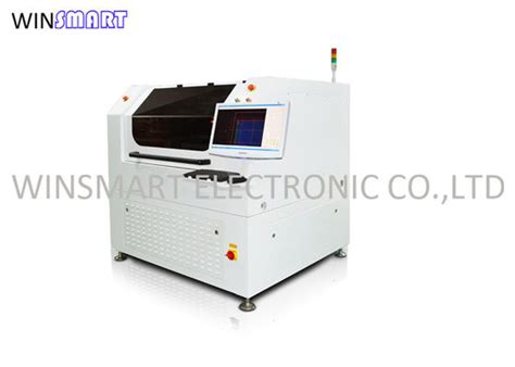
PCB ultraviolet lasers are specialized laser systems that emit light in the ultraviolet spectrum, typically with wavelengths ranging from 355 nm to 405 nm. These lasers are used in various stages of the PCB manufacturing process, including drilling, cutting, and marking. Unlike conventional mechanical drilling or cutting methods, UV lasers offer non-contact processing, eliminating issues like tool wear and breakage.
Advantages of Using PCB Ultraviolet Lasers
- High precision: UV lasers can achieve feature sizes as small as 25 μm, enabling the creation of high-density interconnects and micro-vias.
- Faster processing: With speeds up to 1000 holes per second, UV lasers significantly reduce processing times compared to mechanical drilling.
- Improved reliability: Non-contact processing eliminates the risk of mechanical stress and damage to the PCB, resulting in higher yields and fewer defects.
- Versatility: UV lasers can be used for a wide range of materials, including copper, polyimide, and glass-reinforced epoxy.
Applications of PCB Ultraviolet Lasers
Drilling
One of the primary applications of PCB ultraviolet lasers is drilling micro-vias and through-holes. UV lasers can create high-quality, precise holes with minimal thermal damage to the surrounding material. This is particularly important for high-density interconnect (HDI) PCBs, where the spacing between holes is minimal.
| Parameter | UV Laser Drilling | Mechanical Drilling |
|---|---|---|
| Hole Size | 25 μm – 150 μm | 200 μm and above |
| Speed | Up to 1000 holes/s | 100-300 holes/s |
| Accuracy | ± 5 μm | ± 50 μm |
Cutting
PCB ultraviolet lasers are also used for cutting PCBs into desired shapes and sizes. Laser cutting offers several advantages over mechanical methods, such as higher precision, smoother edges, and the ability to create complex geometries. UV lasers can cut through a variety of PCB materials, including FR-4, polyimide, and flexible substrates.
Marking
UV lasers are ideal for marking PCBs with text, logos, and barcodes. Laser marking is fast, permanent, and requires no consumables, making it a cost-effective solution for PCB identification and traceability. UV lasers can create high-contrast marks on various PCB surface finishes, including silver, gold, and solder mask.
PCB Ultraviolet Laser Technology
Laser Sources
The most common UV laser sources used in PCB manufacturing are solid-state lasers, such as diode-pumped solid-state (DPSS) lasers and fiber lasers. These lasers offer high power, excellent beam quality, and long lifetimes, making them suitable for industrial applications.
-
DPSS Lasers: DPSS lasers use a diode laser to pump a solid-state gain medium, typically neodymium-doped yttrium aluminum garnet (Nd:YAG) or neodymium-doped yttrium orthovanadate (Nd:YVO4). The output wavelength is then converted to the UV range using nonlinear optical processes like frequency doubling or tripling.
-
Fiber Lasers: Fiber lasers use a fiber optic cable doped with rare-earth elements as the gain medium. They offer high efficiency, excellent beam quality, and low maintenance requirements compared to DPSS lasers. UV fiber lasers are becoming increasingly popular in PCB manufacturing due to their compact size and reliability.
Beam Delivery and Focusing
Efficient beam delivery and focusing are critical for achieving high-quality results with PCB ultraviolet lasers. The laser beam is typically guided through a series of mirrors and lenses before being focused onto the PCB surface. The focusing optics determine the spot size and depth of focus, which in turn affect the resolution and accuracy of the process.
-
Galvanometer Scanners: Galvanometer scanners are widely used for high-speed beam positioning in PCB laser processing. They consist of two mirrors mounted on galvanometer motors, which rotate to steer the laser beam across the PCB surface. Galvanometer scanners offer fast scanning speeds and high precision, making them suitable for drilling, cutting, and marking applications.
-
Telecentric Lenses: Telecentric lenses are designed to maintain a constant spot size and focus position over a large working area. They are particularly useful for processing large PCBs or multiple PCBs in a single setup. Telecentric lenses minimize distortion and ensure consistent feature sizes across the entire PCB surface.

Process Control and Optimization
Software and Machine Vision
Advanced software and machine vision systems play a crucial role in optimizing and controlling PCB ultraviolet laser processes. These systems enable real-time monitoring, automatic calibration, and closed-loop feedback control, ensuring consistent and reliable results.
-
CAM Software: Computer-Aided Manufacturing (CAM) software is used to generate the tool paths and process parameters for PCB laser processing. The software takes the PCB design files as input and creates optimized paths for drilling, cutting, and marking operations. Advanced CAM software can also simulate the laser process and detect potential issues before the actual processing begins.
-
Machine Vision: Machine vision systems use cameras and image processing algorithms to inspect the PCB surface before, during, and after laser processing. They can detect and compensate for any misalignment, material variations, or defects, ensuring accurate and consistent results. Machine vision also enables automated quality control, reducing the need for manual inspection and increasing throughput.
Process Parameters
Optimizing the process parameters is essential for achieving the desired results with PCB ultraviolet lasers. The key parameters that affect the process include:
-
Laser Power: The laser power determines the amount of energy delivered to the PCB surface. Higher power levels can increase processing speeds but may also cause thermal damage or debris formation. The optimal power level depends on the material, thickness, and desired feature size.
-
Pulse Duration: The pulse duration, or pulse width, is the time during which the laser is active. Shorter pulses can reduce thermal damage and improve edge quality, while longer pulses may be required for thicker materials or larger feature sizes.
-
Repetition Rate: The repetition rate is the number of laser pulses per second. Higher repetition rates can increase processing speeds but may also lead to heat accumulation and thermal damage. The optimal repetition rate depends on the material, feature size, and desired throughput.
-
Wavelength: The wavelength of the UV laser affects the absorption characteristics of the PCB material. Shorter wavelengths (e.g., 355 nm) are typically used for drilling and cutting, while longer wavelengths (e.g., 405 nm) are suitable for marking and surface modification.
Future Trends and Developments
Shorter Wavelengths
As the demand for smaller feature sizes and higher densities continues to grow, PCB manufacturers are exploring the use of shorter wavelength UV lasers. Deep ultraviolet (DUV) lasers, with wavelengths around 266 nm, offer the potential for even higher resolution and precision compared to current UV laser systems. However, DUV lasers also present challenges in terms of material compatibility, beam delivery, and cost.
Hybrid Laser-Mechanical Processes
Combining UV laser processing with traditional mechanical methods can offer the best of both worlds, leveraging the precision and flexibility of lasers with the speed and cost-effectiveness of mechanical drilling or routing. Hybrid processes can be particularly useful for PCBs with a mix of small and large features, or for applications that require both laser and mechanical processing steps.
Ultrafast Lasers
Ultrafast lasers, with pulse durations in the picosecond or femtosecond range, are emerging as a promising technology for PCB manufacturing. These lasers offer extremely high peak powers and minimal thermal effects, enabling precise material removal and reduced heat-affected zones. Ultrafast lasers can potentially improve the quality and reliability of PCB features, particularly for advanced packaging and high-frequency applications.
Frequently Asked Questions (FAQ)
-
Q: What are the main advantages of using ultraviolet lasers in PCB manufacturing?
A: The main advantages of using UV lasers in PCB manufacturing include high precision, faster processing speeds, improved reliability, and versatility in terms of materials and feature sizes. -
Q: Can PCB ultraviolet lasers be used for both rigid and flexible PCBs?
A: Yes, UV lasers can be used for both rigid and flexible PCBs. They can process a wide range of materials, including FR-4, polyimide, and flexible substrates. -
Q: What is the smallest feature size that can be achieved with PCB ultraviolet lasers?
A: PCB ultraviolet lasers can achieve feature sizes as small as 25 μm, enabling the creation of high-density interconnects and micro-vias. -
Q: How do UV lasers compare to traditional mechanical drilling in terms of speed and accuracy?
A: UV lasers can achieve drilling speeds up to 1000 holes per second, which is significantly faster than mechanical drilling (100-300 holes/s). UV lasers also offer higher accuracy, with a typical tolerance of ±5 μm compared to ±50 μm for mechanical drilling. -
Q: What are the key process parameters that affect the quality and performance of PCB ultraviolet laser processing?
A: The key process parameters include laser power, pulse duration, repetition rate, and wavelength. Optimizing these parameters based on the material, feature size, and desired throughput is essential for achieving high-quality results.
Conclusion
PCB ultraviolet lasers have revolutionized the manufacturing of printed circuit boards, offering numerous advantages over traditional processing methods. With their high precision, fast processing speeds, and versatility, UV lasers have become an essential tool for creating advanced PCBs with high-density interconnects, micro-vias, and complex geometries.
As the electronics industry continues to evolve, PCB manufacturers will increasingly rely on ultraviolet laser technology to meet the growing demands for smaller, faster, and more reliable electronic devices. Ongoing research and development in areas such as shorter wavelengths, hybrid processes, and ultrafast lasers will further expand the capabilities and applications of PCB ultraviolet lasers in the years to come.
By embracing these cutting-edge technologies and optimizing their processes, PCB manufacturers can stay ahead of the curve and deliver the innovative, high-quality products that drive the future of electronics.
No responses yet