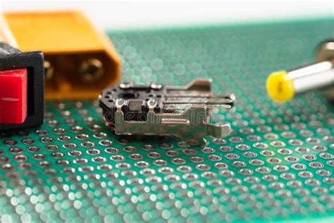
Improper Connector Selection
One of the most common PCB connectivity errors in multi-board systems is improper connector selection. Choosing the right connectors is essential for ensuring reliable electrical and mechanical connections between boards.
Factors to Consider When Selecting Connectors
- Signal Integrity
- Bandwidth Requirements
- Impedance matching
-
Crosstalk reduction
-
Power Delivery
- Current carrying capacity
- Voltage drop
-
Contact resistance
-
Mechanical Robustness
- Mating cycles
- Vibration and shock resistance
-
Locking mechanisms
-
Environmental Factors
- Operating temperature range
- Humidity tolerance
- Sealing against contaminants
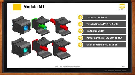
Common Connector Types for Multi-Board Systems
| Connector Type | Description | Advantages | Disadvantages |
|---|---|---|---|
| Board-to-Board | Direct connection between boards | Compact, low-cost | Limited flexibility, difficult to separate boards |
| Card-Edge | PCB edge inserted into a socket | Simple, cost-effective | Limited contact density, wear over time |
| Mezzanine | Stacked boards with connectors | High-density, modular design | Increased height, potential signal integrity issues |
| Backplane | Motherboard with daughter cards | Scalable, hot-swappable | Complex design, signal integrity challenges |
To avoid connector selection errors, consider the following best practices:
- Carefully evaluate system requirements and choose connectors that meet the electrical, mechanical, and environmental needs.
- Consult connector manufacturer datasheets and application notes for guidance on proper selection and usage.
- Perform Signal integrity simulations and power delivery analysis to validate connector performance.
- Conduct mechanical stress tests to ensure connector reliability under expected operating conditions.
Incorrect Impedance Matching
Incorrect impedance matching is another common PCB connectivity error that can lead to signal integrity issues in multi-board systems. Proper impedance matching is crucial for minimizing reflections and ensuring clean signal transmission between boards.
Importance of Impedance Matching
- Reduces signal reflections and distortions
- Improves signal quality and timing
- Minimizes electromagnetic interference (EMI)
- Enables higher data rates and longer transmission distances
Factors Affecting Impedance Matching
- PCB stackup
- Dielectric material properties
- Layer thicknesses
-
Copper weight and trace geometry
-
Trace Routing
- Trace width and spacing
- Microstrip vs. stripline routing
-
Discontinuities (vias, bends, etc.)
-
Termination Strategies
- Series termination
- Parallel termination
- AC termination
To ensure proper impedance matching, follow these guidelines:
- Design PCB stackups with controlled impedance in mind, considering material properties and layer configurations.
- Use Impedance Calculators or field solvers to determine appropriate trace widths and spacings for target impedances.
- Minimize discontinuities in trace routing and use gradual bends instead of sharp corners.
- Implement appropriate termination strategies based on signal characteristics and system requirements.
- Perform time-domain reflectometry (TDR) measurements to validate impedance matching and identify any issues.
Inadequate Power Integrity
Inadequate power integrity is a critical PCB connectivity error that can cause system instability, performance degradation, and even component failure. Proper power delivery and decoupling are essential for maintaining clean and stable power supplies to all components in a multi-board system.
Power Distribution Network (PDN) Design Considerations
- Power Supply Partitioning
- Separate analog and digital power domains
- Isolate noise-sensitive circuits
-
Use local power regulation for sensitive components
-
Plane Capacitance
- Leverage power and ground planes for intrinsic capacitance
- Minimize plane splits and perforations
-
Maintain sufficient plane area for current carrying capacity
-
Decoupling Capacitor Placement
- Place decoupling capacitors close to power consumers
- Use a mix of capacitor values for broadband decoupling
-
Minimize loop inductance through proper placement and routing
-
Via Optimization
- Use sufficient via sizes and quantities for low impedance connections
- Minimize via inductance through proper placement and stackup design
- Consider blind and buried vias for dense designs
To mitigate power integrity issues, consider the following best practices:
- Perform early PDN simulations to identify potential issues and optimize designs.
- Use power integrity analysis tools to assess voltage drops, current densities, and impedance profiles.
- Follow recommended decoupling strategies and placement guidelines from component manufacturers.
- Implement proper grounding techniques, such as star grounding or multi-point grounding, based on system requirements.
- Conduct power integrity measurements, such as impedance spectroscopy or voltage ripple analysis, to validate PDN performance.

FAQs
-
Q: What are the most common connectors used for multi-board PCB systems?
A: Common connectors for multi-board PCB systems include board-to-board, card-edge, mezzanine, and backplane connectors. The choice depends on factors such as signal integrity, power delivery, mechanical robustness, and environmental requirements. -
Q: Why is impedance matching important in multi-board PCB connectivity?
A: Impedance matching is crucial for minimizing signal reflections, improving signal quality, and reducing electromagnetic interference (EMI) in multi-board PCB systems. Proper impedance matching enables clean signal transmission between boards and supports higher data rates and longer transmission distances. -
Q: How can I ensure proper power integrity in a multi-board PCB system?
A: To ensure proper power integrity, consider partitioning power supplies, leveraging plane capacitance, placing decoupling capacitors close to power consumers, optimizing via placement and sizes, and following recommended grounding techniques. Performing PDN simulations and measurements can help identify and mitigate power integrity issues. -
Q: What are the consequences of poor PCB connectivity in multi-board systems?
A: Poor PCB connectivity can lead to various issues, such as signal integrity problems, power delivery failures, system instability, performance degradation, and even component damage. These issues can compromise the functionality, reliability, and overall performance of the multi-board system. -
Q: How can I avoid PCB connectivity errors in multi-board systems?
A: To avoid PCB connectivity errors, follow best practices such as careful connector selection, proper impedance matching, and robust power integrity design. Perform simulations, analyses, and measurements to validate connectivity performance and identify any issues early in the design process. Consult manufacturer guidelines and application notes for specific recommendations.
Conclusion
Multi-board PCB connectivity errors can have severe consequences on system functionality, reliability, and performance. By understanding and addressing the top three connectivity errors – improper connector selection, incorrect impedance matching, and inadequate power integrity – designers can create robust and reliable multi-board systems.
To mitigate these errors, it is essential to follow best practices in connector selection, impedance matching, and power integrity design. Performing simulations, analyses, and measurements throughout the design process can help identify and resolve connectivity issues early on.
By paying close attention to PCB connectivity and implementing the strategies discussed in this article, designers can ensure that their multi-board systems meet the desired electrical, mechanical, and environmental requirements, ultimately leading to successful and reliable products.
No responses yet