
Introduction to PCB stackups
A printed circuit board (PCB) stackup refers to the arrangement of copper and insulating layers that make up a PCB. The stackup defines the number of layers, their order, and the materials used for each layer. Choosing the right PCB stackup is crucial for ensuring proper functionality, signal integrity, and manufacturability of the PCB.
In this article, we will focus on the 4 layer PCB stackup, which is a common configuration used in many electronic designs. We’ll explore the basics of 4 layer stackups, their advantages, and best practices for designing them effectively.
What is a 4 Layer PCB Stackup?
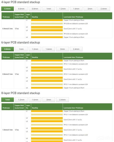
A 4 layer PCB stackup consists of four conductive copper layers separated by three insulating layers. The typical arrangement of a 4 layer stackup is as follows:
| Layer | Description |
|---|---|
| Top Layer | Signal layer, component placement |
| Prepreg | Insulating layer |
| Inner Layer 1 | Power or ground plane |
| Core | Insulating layer |
| Inner Layer 2 | Power or ground plane |
| Prepreg | Insulating layer |
| Bottom Layer | Signal layer, component placement |
The top and bottom layers are typically used for signal routing and component placement. The inner layers are usually dedicated to power and ground planes, providing a stable reference for the signal layers and reducing electromagnetic interference (EMI).
Advantages of 4 Layer PCB stackups
Using a 4 layer PCB stackup offers several advantages over 2 layer boards:
-
Improved signal integrity: The dedicated power and ground planes in a 4 layer stackup provide a low-impedance return path for signals, reducing crosstalk and EMI.
-
Better power distribution: The inner power and ground planes ensure a more uniform power distribution across the board, minimizing voltage drops and improving overall power integrity.
-
Increased routing space: With four layers available, there is more space for routing signals, allowing for higher component density and more complex designs.
-
Enhanced mechanical stability: The additional layers in a 4 layer stackup make the board more rigid and less prone to warping or bending.
Choosing the Right Materials for Your 4 Layer PCB Stackup
When designing a 4 layer PCB stackup, selecting the appropriate materials is essential for achieving the desired performance and reliability. The main materials to consider are:
-
Copper: The thickness and weight of the copper foil used for each layer affects the signal integrity, current carrying capacity, and manufacturability of the board. Common copper weights include 0.5 oz, 1 oz, and 2 oz.
-
Laminate: The core and prepreg materials used as insulators between layers impact the dielectric constant, dissipation factor, and thermal properties of the board. Popular laminate materials include FR-4, Rogers, and Isola.
-
Solder mask: The solder mask layer protects the copper traces from oxidation and prevents short circuits during soldering. It also provides a visual reference for component placement.
-
Silkscreen: The silkscreen layer is used for labeling components, test points, and other information on the board, making it easier to assemble and debug the PCB.
Designing Your 4 Layer PCB Stackup
When creating a 4 layer PCB stackup, follow these best practices to ensure optimal performance and manufacturability:
Define the Layer Stack Order
Determine the order of the layers based on your design requirements. A common arrangement for a 4 layer stackup is:
| Layer | Description |
|---|---|
| Layer 1 (Top) | Signal layer, component placement |
| Layer 2 | Ground plane |
| Layer 3 | Power plane |
| Layer 4 (Bottom) | Signal layer, component placement |
This arrangement provides a good balance between signal integrity and power distribution. However, you may need to adjust the layer order depending on your specific design needs, such as high-speed signals or multiple power domains.
Choose the Right Copper Weight
Select the appropriate copper weight for each layer based on the current carrying requirements and signal integrity needs. Some guidelines for choosing copper weights are:
| Layer | Copper Weight |
|---|---|
| Signal Layers | 0.5 oz or 1 oz |
| Power and Ground Planes | 1 oz or 2 oz |
Using a heavier copper weight for power and ground planes improves their current carrying capacity and reduces voltage drops. For signal layers, a lighter copper weight is often sufficient and can help minimize the overall thickness of the board.
Define the Layer Spacing
Determine the spacing between layers based on the dielectric constant of the insulating material and the desired impedance of the traces. A general rule of thumb is to keep the spacing between signal layers and their adjacent planes consistent to maintain a uniform impedance throughout the board.
For example, if using FR-4 laminate with a dielectric constant of 4.5, you might use the following layer spacing:
| Layer Spacing | Thickness |
|---|---|
| Prepreg (between Top Layer and Inner Layer 1) | 7.62 mils |
| Core (between Inner Layers) | 47 mils |
| Prepreg (between Bottom Layer and Inner Layer 2) | 7.62 mils |
Route Signals Properly
When routing signals on the top and bottom layers, follow these guidelines:
– Keep signal traces as short and direct as possible to minimize inductance and reduce signal reflections.
– Avoid routing signals parallel to each other for long distances to reduce crosstalk.
– Use appropriate trace widths based on the current carrying requirements and impedance targets.
– Provide adequate clearance between traces and component pads to prevent short circuits.
Optimize Power and Ground Planes
To ensure optimal power distribution and signal integrity, follow these best practices for power and ground planes:
- Use solid planes instead of gridded planes to provide a low-impedance return path for signals.
- Avoid splitting power and ground planes unnecessarily, as this can create discontinuities and degrade signal quality.
- Provide sufficient decoupling capacitors between power and ground planes to minimize voltage ripple and noise.
- Use appropriate via sizes and spacing to connect power and ground planes to their respective components and signal layers.

FAQ
1. What is the difference between a 4 layer and 2 layer PCB stackup?
A 4 layer PCB stackup has four conductive copper layers separated by three insulating layers, while a 2 layer stackup has only two copper layers with one insulating layer between them. 4 layer stackups offer better signal integrity, power distribution, and routing space compared to 2 layer boards.
2. Can I use different materials for the core and prepreg layers in a 4 layer PCB stackup?
Yes, you can use different materials for the core and prepreg layers, depending on your design requirements. For example, you might use a high-performance material like Rogers for the core layer to achieve better signal integrity, and a standard FR-4 material for the prepreg layers to reduce cost.
3. How do I determine the appropriate trace width and spacing for my 4 layer PCB?
The trace width and spacing depend on several factors, such as the signal frequency, current carrying requirements, and the manufacturing capabilities of your PCB fabricator. You can use online calculators or consult with your fabricator to determine the appropriate trace width and spacing for your design.
4. What are the typical layer thicknesses for a 4 layer PCB stackup?
The typical layer thicknesses for a 4 layer PCB stackup using FR-4 laminate are:
| Layer | Thickness |
|---|---|
| Copper (signal layers) | 1.4 mils (1 oz) |
| Copper (power/ground planes) | 2.8 mils (2 oz) |
| Prepreg | 7.62 mils |
| Core | 47 mils |
However, these thicknesses can vary depending on the specific materials used and the design requirements.
5. Can I have more than one power or ground plane in a 4 layer PCB stackup?
Yes, you can have multiple power or ground planes in a 4 layer PCB stackup, depending on your design needs. For example, you might have separate power planes for analog and digital circuits, or multiple ground planes for different Signal Return Paths. However, keep in mind that adding more planes will increase the overall thickness and cost of the board.
Conclusion
A well-designed 4 layer PCB stackup is essential for ensuring the proper functionality, signal integrity, and manufacturability of your electronic design. By understanding the basics of 4 layer stackups, choosing the right materials, and following best practices for layer arrangement, signal routing, and power distribution, you can create reliable and high-performance PCBs that meet your design requirements.
Remember to work closely with your PCB fabricator throughout the design process to ensure that your stackup is manufacturable and cost-effective. With careful planning and attention to detail, you can unlock the full potential of 4 layer PCB stackups for your next project.
No responses yet