How Does Surface Mount Technology Work?
The SMT component placement process includes these key steps:
-
Solder Paste Stenciling – A thin stainless steel stencil with precision laser-cut apertures that match the solder pads on the PCB is aligned over the board. Solder paste is then spread over the stencil with a blade, forcing it through the cut openings and depositing it on the pads.
-
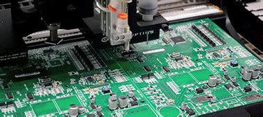
Pick and Place – A robotic pick and place machine, usually with multiple nozzles/heads, picks up the SMT components from tape reels, tubes, or trays and places them on their designated locations on the PCB at a very high speed. The components are held in place by the tackiness of the solder paste.
-
Reflow Soldering – After placement, the PCBs are passed through an oven that heats the board to a temperature above the melting point of the solder, typically above 200°C. The solder paste reflows in a molten state and forms solder joints between component leads and the pads on the PCB. As the solder cools, it solidifies and creates a strong mechanical and electrical connection.
-
Inspection – Automatic optical inspection (AOI) is commonly used after reflow to check for missing components, misalignments, insufficient solder, or solder bridging. X-ray inspection may also be used to inspect solder joints underneath packages like ball grid arrays (BGAs).
Solder Paste Stenciling
The solder paste used for SMT is made of powdered solder suspended in a thick medium called flux. The composition is usually around 96.5% metal powder and 3.5% flux by weight. The metal portion is usually a eutectic or near-eutectic alloy of tin, lead, and sometimes silver. Lead-free solders are also widely used now.
The key properties of solder paste are:
- Printability – Ability to be printed through the stencil apertures without slumping or sticking.
- Tackiness – Ability to hold components in place after placement.
- Viscosity – Needs to be low enough to flow easily but high enough to retain its shape after printing.
- Flux Activity – The flux must be active enough to clean the component leads and PCB pads to allow good wetting during reflow.
Stainless steel SMT Stencils typically range from 0.10 mm (0.004″) to 0.20 mm (0.008″) in thickness. The aperture sizes and shapes are designed to match the footprint of the SMT pads on the PCB. Solder paste is applied using a metal blade or squeegee that forces the paste through the stencil apertures as it is dragged across the surface of the stencil.
Pick and Place
Modern pick and place machines are highly sophisticated and can place components as small as 0.25 mm x 0.125 mm at speeds up to 136,000 cph (components per hour) or more. They use vacuum nozzles to pick up the components and high resolution cameras to identify and align the components with the PCB.
The main types of feeders for SMT components are:
- Tape and Reel – Components are packaged in pockets of a plastic carrier tape which is wound onto a reel. The cover tape is peeled back to expose the components. This is the most common method.
- Tube Feeders – Cylindrical components like resistors and diodes are loaded into plastic tubes. The tubes are fed into the machine and the components are pushed out one at a time.
- Tray Feeders – Components like BGAs and QFPs are supplied in plastic trays. The trays are stacked in a feeder unit and the pick and place head accesses each component through an open slot in the cover tape.
The placement accuracy of SMT pick and place machines is typically +/-0.05 mm or better. Some machines also have on-board solder paste dispensers and selective soldering heads for applying and reflowing solder on specific areas of the board.
Reflow Soldering
Reflow soldering in SMT is done by passing the entire PCB through an oven that follows a precise temperature profile that brings the solder paste through four stages:
- Preheat – The board is slowly heated to 150-180°C to activate the flux and drive off volatile solvents.
- Thermal Soak – The temperature is held steady to allow the components and board to reach an even temperature and to allow the flux to clean the surfaces.
- Reflow – The temperature is rapidly raised above the melting point of the solder, typically to a peak of 220-250°C. The solder paste melts and forms solder joints between the component leads and PCB pads.
- Cooling – The board is cooled, allowing the solder to solidify into reliable solder joints.
The reflow oven may use convection (hot air), infrared radiation, or a combination of both to heat the board. The temperature profile must be carefully controlled to ensure the solder melts completely but the components are not damaged by excessive heat.
Inspection
After reflow, the solder joints are inspected to ensure a good electrical and mechanical connection has been made. Automatic optical inspection (AOI) systems use high resolution cameras and pattern recognition software to check for defects like:
- Missing components
- Misaligned components
- Insufficient solder
- Solder bridges or short circuits
- Tombstoning (one end of a component lifts off the pad)
X-ray inspection may also be used, especially for hidden solder joints like those under a BGA package. The X-ray image will show voids, shorts, and other defects in the solder balls that are not visible optically.
Advantages of Surface Mount Technology
SMT has revolutionized electronics manufacturing and has many advantages over through-hole technology:
Smaller Size
SMT components are much smaller than their through-hole counterparts – often less than half the size. This allows for much higher component density on the PCB, which leads to smaller overall product sizes. It’s one of the main reasons why modern electronics like smartphones can pack so much functionality into such a small space.
Lower Cost
Although the initial setup costs for SMT can be higher due to the need for specialized equipment, the overall cost per unit is typically lower in volume production. This is because:
- SMT components are generally cheaper than through-hole
- Placement and soldering can be fully automated
- Fewer drilling and through-hole plating steps are needed
- PCBs can be smaller and simpler
Faster Assembly
SMT allows for very high speed automated assembly. Modern SMT Lines can place components at speeds of over 100,000 per hour per machine. Through-hole components usually need to be inserted manually or with slower, dedicated insertion machines.
Better Performance
SMT allows for smaller packages with shorter lead lengths, which reduces parasitic inductance and capacitance. This can lead to better high-frequency performance in applications like RF and high-speed digital circuits.
More Reliable
When done properly, SMT solder joints are at least as reliable as through-hole joints. The smaller size and lack of through-holes also makes SMT PCBs more resistant to shock and vibration.

Disadvantages of Surface Mount Technology
Despite its many advantages, SMT does have some limitations and challenges:
Component Handling
SMT components can be very small and fragile, making them difficult to handle manually. Special equipment and a skilled operator are needed for prototype or small volume assembly.
Thermal Stress
SMT components are subjected to more thermal stress during reflow soldering than through-hole components during wave soldering. Careful control of the reflow profile is needed to avoid damage, especially to sensitive components like electrolytic capacitors and connectors.
Inspection and Repair
Some SMT solder joints, like those under a BGA, can’t be inspected visually. X-ray systems may be needed. If a defective component is found, removing and replacing it can be difficult and may damage the PCB. Specialized rework stations with hot air nozzles and vacuum tweezers are used.
Mechanical Stress
SMT components are held on only by the solder joints, unlike through-hole components which are physically anchored by their leads. This makes SMT assemblies more susceptible to damage from mechanical stress, especially larger/heavier components. Proper design of the PCB and enclosure is important to minimize flexing and vibration.

Frequently Asked Questions
Q: What are the most common SMT packages?
A: Some of the most common SMT packages are:
– Chip resistors and capacitors
– Small outline integrated circuits (SOIC)
– Quad flat packages (QFP)
– Ball grid arrays (BGA)
– Land grid arrays (LGA)
– Quad flat no-leads (QFN)
Q: Can through-hole and SMT components be mixed on one PCB?
A: Yes, it’s common to have a mix of SMT and through-hole components on the same PCB, especially for connectors, large capacitors, transformers, and other components that aren’t available or suitable for SMT. The through-hole components are usually soldered by hand or with a selective wave soldering machine after the SMT process.
Q: What is the smallest size SMT component?
A: The smallest standard chip size is 0201 (0.02″ x 0.01″, or 0.5mm x 0.25mm). Even smaller 01005 (0.4mm x 0.2mm) chips are sometimes used. However, these are very challenging to place and solder and are only used when absolutely necessary.
Q: What is the difference between lead-based and lead-free solder paste?
A: Traditional solder paste contains a tin-lead alloy, usually 63% tin and 37% lead (Sn63/Pb37). However, due to health and environmental concerns, lead-based solders are being phased out in many countries. Lead-free solders use tin alloyed with silver, copper, or bismuth instead. Lead-free solders generally have a higher melting point (217-227°C vs 183°C for leaded) and may require changes to the reflow profile and PCB design for optimal results.
Q: Can SMT be used for high-power applications?
A: Yes, but special considerations are needed. Higher power SMT components like MOSFETs and voltage regulators generate significant heat and need a large thermal pad to dissipate it to the PCB. The PCB may need thicker copper, more vias, or even a metal core to handle the heat. Components may also need an external heat sink. Proper thermal design and testing is critical for reliability in high-power SMT applications.

No responses yet