What is Solder Mask?
Solder mask is a polymer-based coating that is applied to the copper traces of a PCB. Its primary purpose is to prevent solder from bridging between the copper traces during the soldering process, which could lead to short circuits and other electrical issues. Solder mask also serves as an insulating layer, protecting the copper traces from damage and oxidation.
Composition of Solder Mask
Solder mask is typically composed of a photosensitive polymer resin, along with various additives such as pigments, fillers, and hardeners. The most common polymers used in solder mask formulations are:
- Epoxy-based resins
- Acrylic-based resins
- Polyurethane-based resins
- Polyimide-based resins
These polymers are chosen based on their specific properties, such as chemical resistance, thermal stability, and adhesion to the PCB substrate.
Types of Solder Mask
There are two main types of solder mask: liquid photoimageable (LPI) and dry film photoimageable (DFPI).
-
Liquid Photoimageable (LPI) Solder Mask: LPI solder mask is a liquid coating that is applied to the PCB using various methods, such as screen printing, spraying, or curtain coating. After application, the solder mask is exposed to UV light through a photomask, which selectively cures the exposed areas. The uncured areas are then developed and removed, leaving the desired solder mask pattern on the PCB.
-
Dry Film Photoimageable (DFPI) Solder Mask: DFPI solder mask is a solid film that is laminated onto the PCB surface using heat and pressure. Like LPI solder mask, DFPI is exposed to UV light through a photomask and developed to create the desired pattern. DFPI solder mask is generally thicker and more durable than LPI solder mask, making it suitable for high-reliability applications.
Solder Mask Application Methods
The choice of solder mask application method depends on factors such as the type of solder mask, the desired thickness, and the production volume. The most common application methods are:
-
Screen Printing: A mesh screen with the desired solder mask pattern is used to transfer the liquid solder mask onto the PCB surface. This method is suitable for low to medium production volumes and can achieve a thickness of 0.5 to 2 mils (12.7 to 50.8 microns).
-
Spraying: Liquid solder mask is sprayed onto the PCB surface using a spray gun. This method is suitable for low to medium production volumes and can achieve a thickness of 0.5 to 2 mils (12.7 to 50.8 microns).
-
Curtain Coating: Liquid solder mask is poured onto the PCB surface and distributed evenly using a curtain coater. This method is suitable for high production volumes and can achieve a thickness of 0.5 to 2 mils (12.7 to 50.8 microns).
-
Dry Film Lamination: DFPI solder mask is laminated onto the PCB surface using heat and pressure. This method is suitable for high-reliability applications and can achieve a thickness of 1 to 4 mils (25.4 to 101.6 microns).

Essential Properties of Solder Mask
To ensure optimal performance, solder mask must possess several key properties:
-
Adhesion: Solder mask must adhere well to the PCB substrate and copper traces to prevent delamination and ensure long-term reliability.
-
Electrical Insulation: Solder mask must provide adequate electrical insulation between the copper traces to prevent short circuits and other electrical issues.
-
Chemical Resistance: Solder mask must be resistant to various chemicals used in the PCB manufacturing process, such as flux, solvents, and cleaning agents.
-
Thermal Stability: Solder mask must be able to withstand the high temperatures encountered during the soldering process without degrading or losing its properties.
-
UV Resistance: Solder mask must be resistant to UV light to prevent degradation and discoloration over time.
-
Flexibility: Solder mask must be flexible enough to withstand the stresses and strains encountered during the PCB assembly process and in the final application.
-
Resolution: Solder mask must be capable of achieving high-resolution patterns to accommodate the increasingly fine features and pitch sizes in modern PCB designs.

Solder Mask Colors and Legends
Solder mask is available in a variety of colors, with green being the most common. Other popular colors include blue, red, yellow, black, and white. The choice of solder mask color is often dictated by the specific application or customer preference.
In addition to solid colors, solder mask can also be used to create legends or markings on the PCB surface. Legends are typically used to identify components, test points, or other important features on the PCB. They can be created by selectively exposing and developing the solder mask to reveal the underlying copper or by printing the legend using a secondary process such as silk screening.

Solder Mask and PCB Surface Finishes
Solder mask is often used in conjunction with various PCB surface finishes, which are applied to the exposed copper areas to improve solderability, protect against oxidation, and enhance the overall reliability of the PCB. Some common PCB surface finishes include:
-
Hot Air Solder Leveling (HASL): A tin-lead alloy is applied to the exposed copper areas and leveled using hot air to create a smooth, solderable surface.
-
Electroless Nickel Immersion Gold (ENIG): A layer of electroless nickel is deposited onto the exposed copper, followed by a thin layer of immersion gold. ENIG provides excellent solderability and shelf life.
-
Immersion Silver: A thin layer of silver is deposited onto the exposed copper, providing good solderability and lower cost compared to ENIG.
-
Immersion Tin: A thin layer of tin is deposited onto the exposed copper, offering good solderability and low cost.
Solder Mask and Controlled Impedance
In high-speed PCB designs, controlling the impedance of the transmission lines is critical for maintaining signal integrity. Solder mask plays an essential role in achieving controlled impedance by providing a consistent dielectric layer between the copper traces and the surrounding environment.
The dielectric constant (Dk) and loss tangent (Df) of the solder mask material, along with its thickness, are key factors in determining the impedance of the transmission lines. PCB designers must work closely with solder mask suppliers to select the appropriate material and thickness to meet the specific impedance requirements of their design.
Solder Mask and Manufacturing Considerations
When incorporating solder mask into a PCB design, several manufacturing considerations must be taken into account:
-
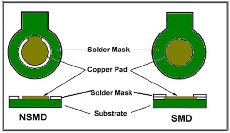
Solder Mask Clearance: Adequate clearance must be provided between the solder mask and the copper traces to ensure proper adhesion and to prevent solder bridging. The minimum clearance is typically 3 to 5 mils (76.2 to 127 microns), depending on the solder mask type and application method.
-
Solder Mask Expansion: During the curing process, solder mask may expand slightly, which can cause misalignment or encroachment onto the copper traces. PCB designers must account for this expansion when creating the solder mask artwork.
-
Solder Mask Registration: Accurate registration between the solder mask and the copper traces is essential for ensuring proper insulation and preventing short circuits. PCB manufacturers use various methods, such as fiducial marks or registration holes, to align the solder mask with the underlying copper features.
-
Solder Mask Thickness: The thickness of the solder mask can impact its performance and manufacturability. Thinner solder masks may be more prone to defects or incomplete coverage, while thicker solder masks may be more challenging to apply and cure consistently.
Solder Mask and Environmental Considerations
As with all aspects of PCB manufacturing, solder mask materials and processes must comply with various environmental regulations and standards. Some key considerations include:
-
RoHS Compliance: Solder mask materials must be free of restricted substances, such as lead, cadmium, and hexavalent chromium, to comply with the European Union’s Restriction of Hazardous Substances (RoHS) directive.
-
REACH Compliance: Solder mask materials must also comply with the European Union’s Registration, Evaluation, Authorization, and Restriction of Chemicals (REACH) regulation, which aims to improve the protection of human health and the environment from the risks posed by chemicals.
-
Halogen-Free: Some applications, particularly in the automotive and aerospace industries, require the use of halogen-free solder mask materials to reduce the risk of toxic gas emissions in the event of a fire.
-
VOC Emissions: Solder mask materials and processes must be designed to minimize the emission of volatile organic compounds (VOCs), which can contribute to air pollution and pose health risks to workers.
Frequently Asked Questions (FAQ)
-
What is the difference between solder mask and conformal coating?
Solder mask is a permanent coating applied to the PCB surface to prevent solder from adhering to unwanted areas during the soldering process. Conformal coating, on the other hand, is a removable coating applied after the soldering process to protect the PCB from environmental factors such as moisture, dust, and chemicals. -
Can solder mask be removed?
Solder mask is designed to be a permanent coating and is not easily removed. However, in some cases, solder mask can be removed using chemical or mechanical methods, such as abrasive blasting or laser ablation. These methods should be used with caution, as they can damage the underlying PCB if not performed correctly. -
What is the typical thickness of solder mask?
The typical thickness of solder mask ranges from 0.5 to 2 mils (12.7 to 50.8 microns) for LPI solder mask and 1 to 4 mils (25.4 to 101.6 microns) for DFPI solder mask. The specific thickness required depends on factors such as the PCB design, the desired electrical and mechanical properties, and the manufacturing process. -
Can solder mask be used on flexible PCBs?
Yes, solder mask can be used on flexible PCBs, but special considerations must be taken into account. Flexible solder mask materials, such as polyimide-based resins, are typically used to accommodate the bending and flexing of the PCB. The application process may also need to be modified to ensure proper adhesion and coverage on the flexible substrate. -
How does solder mask affect the assembly process?
Solder mask plays a critical role in the PCB assembly process by preventing solder from adhering to unwanted areas and ensuring proper insulation between the copper traces. The quality and consistency of the solder mask can impact the reliability and yield of the assembled PCB. Proper solder mask design and application are essential for achieving a successful assembly process.
In conclusion, solder mask is a vital component in the manufacturing of PCBs, providing essential protection, insulation, and aesthetic benefits. Understanding the various aspects of solder mask material, including its composition, types, application methods, and essential properties, is crucial for designing and manufacturing high-quality, reliable PCBs. As PCB technology continues to evolve, solder mask materials and processes must also adapt to meet the ever-increasing demands of the electronics industry.
| Property | LPI Solder Mask | DFPI Solder Mask |
|---|---|---|
| Composition | Liquid photoimageable polymer resin | Solid photoimageable film |
| Application Method | Screen printing, spraying, curtain coating | Dry film lamination |
| Typical Thickness | 0.5 to 2 mils (12.7 to 50.8 microns) | 1 to 4 mils (25.4 to 101.6 microns) |
| Advantages | Suitable for low to medium production volumes, easier to apply | Suitable for high-reliability applications, more durable |
| Disadvantages | Less durable than DFPI, may have inconsistencies in coverage | More expensive, requires specialized equipment for lamination |
No responses yet