Introduction to Solder Mask
Solder mask, also known as solder resist or solder stop, is a vital component in the manufacturing of printed circuit boards (PCBs). This protective layer is applied to the copper traces of a PCB to prevent accidental short circuits and to protect the copper from oxidation and other environmental factors. Solder mask also provides a surface for the application of solder paste and components during the assembly process.
What is Solder Mask Made Of?
Solder mask is typically made of a polymer material that is applied as a liquid or film to the PCB surface. The most common types of solder mask materials are:
-
Liquid Photoimageable Solder Mask (LPSM): This type of solder mask is applied as a liquid and then exposed to UV light through a photomask to cure and harden in the desired pattern.
-
Dry Film Photoimageable Solder Mask (DFSM): This type of solder mask is applied as a dry film and then exposed to UV light through a photomask to cure and harden in the desired pattern.
-
Liquid Photoimageable Solder Mask (LPI): This type of solder mask is similar to LPSM but is applied using a screen printing process instead of a photomask.
Properties of Solder Mask
Solder mask has several important properties that make it suitable for use in PCBs:
-
Electrical Insulation: Solder mask provides electrical insulation between the copper traces and prevents short circuits.
-
Chemical Resistance: Solder mask is resistant to a wide range of chemicals, including acids, alkalis, and solvents.
-
Thermal Resistance: Solder mask can withstand high temperatures during the soldering process without degrading or losing its protective properties.
-
Mechanical Protection: Solder mask provides a protective layer that helps to prevent damage to the copper traces during handling and assembly.
Solder Mask Application Process
The application of solder mask to a PCB involves several steps:
-
Cleaning: The PCB surface is cleaned to remove any contaminants or residues that could affect the adhesion of the solder mask.
-
Solder Mask Application: The solder mask material is applied to the PCB surface using one of the methods described above (LPSM, DFSM, or LPI).
-
Exposure: The solder mask is exposed to UV light through a photomask or screen to cure and harden in the desired pattern.
-
Developing: The unexposed areas of the solder mask are removed using a developing solution, leaving only the cured solder mask on the PCB surface.
-
Curing: The PCB is heated to fully cure the solder mask and ensure a strong bond to the copper traces.
Solder Mask Colors
Solder mask is available in a range of colors, with green being the most common. Other colors include blue, red, yellow, black, and white. The choice of color is often based on aesthetic preferences or to provide contrast with the copper traces and components.

Advantages of Using Solder Mask
Using solder mask in PCB manufacturing provides several advantages:
-
Improved Reliability: Solder mask helps to prevent short circuits and other failures that can occur due to accidental contact between copper traces or exposure to environmental factors.
-
Enhanced Manufacturability: Solder mask provides a surface for the application of solder paste and components during the assembly process, making it easier to place and solder components accurately.
-
Increased Durability: Solder mask provides a protective layer that helps to prevent damage to the copper traces during handling and use, improving the overall durability of the PCB.
-
Better Aesthetics: Solder mask can be used to create a professional and aesthetically pleasing appearance for the PCB, with a range of colors available to suit different design preferences.

Disadvantages of Using Solder Mask
While solder mask provides many benefits in PCB manufacturing, there are also some potential disadvantages to consider:
-
Increased Cost: The application of solder mask adds an additional step to the PCB manufacturing process, which can increase the overall cost of the PCB.
-
Reduced Thermal Conductivity: Solder mask can act as a thermal insulator, reducing the ability of the PCB to dissipate heat. This can be a concern for high-power or high-frequency applications.
-
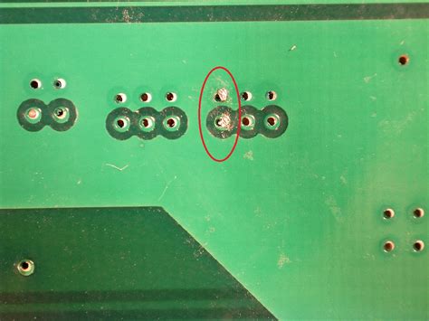
Potential for Defects: If the solder mask is not applied properly or if there are defects in the solder mask material, it can lead to problems such as poor adhesion, bubbles, or pinholes that can compromise the protective properties of the solder mask.

Solder Mask Design Considerations
When designing a PCB that will use solder mask, there are several factors to consider:
-
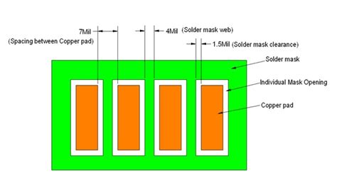
Clearance: There should be sufficient clearance between the copper traces and the solder mask opening to ensure that the solder mask does not interfere with the soldering process.
-
Solder Mask Expansion: Solder mask can expand during the curing process, so it is important to account for this expansion when designing the PCB layout.
-
Solder Mask Thickness: The thickness of the solder mask can affect its protective properties and the ability to apply solder paste and components. A typical solder mask thickness is between 0.5 and 1.0 mils (0.0127 to 0.0254 mm).
-
Solder Mask Color: The choice of solder mask color can affect the visibility of the copper traces and components, as well as the overall appearance of the PCB.
Frequently Asked Questions (FAQ)
- What is the purpose of solder mask on a PCB?
-
Solder mask serves as a protective layer for the copper traces on a PCB, preventing short circuits, oxidation, and other environmental damage. It also provides a surface for applying solder paste and components during the assembly process.
-
Is solder mask required on all PCBs?
-
While solder mask is not strictly required on all PCBs, it is highly recommended for most applications. PCBs without solder mask are more susceptible to damage and may be more difficult to assemble.
-
Can solder mask be removed from a PCB?
-
Yes, solder mask can be removed from a PCB using various methods such as chemical stripping or mechanical abrasion. However, removing the solder mask can compromise the protection of the copper traces and is not recommended unless necessary for repair or modification.
-
What is the difference between LPSM and DFSM solder mask?
-
LPSM (Liquid Photoimageable Solder Mask) is applied as a liquid and then exposed to UV light through a photomask to cure and harden in the desired pattern. DFSM (Dry Film Photoimageable Solder Mask) is applied as a dry film and then exposed to UV light through a photomask to cure and harden in the desired pattern.
-
Can solder mask be used on flexible PCBs?
- Yes, solder mask can be used on flexible PCBs, but the choice of solder mask material and application process may need to be adapted to account for the flexibility of the substrate. Special flexible solder mask materials are available for this purpose.
Conclusion
Solder mask is an essential component in the manufacturing of PCBs, providing a protective layer for the copper traces and a surface for the application of solder paste and components. By understanding the properties, application process, and design considerations for solder mask, PCB Designers and manufacturers can create reliable, durable, and aesthetically pleasing PCBs for a wide range of applications.

No responses yet