What is Surface Mount Technology (SMT)?
Surface Mount Technology (SMT) is a method for constructing electronic circuits where the components are mounted directly onto the surface of a printed circuit board (PCB). SMT has largely replaced the through-hole technology construction method of fitting components with wire leads into holes in the PCB.
SMT components are usually smaller than their through-hole counterparts. It’s become the standard way of making most electronics today and is used in everything from computers and communications equipment to consumer electronics and medical devices.
Advantages of SMT
- Smaller components and higher component density, allowing more compact and lightweight products
- Fewer holes need to be drilled through PCBs
- Components can be placed on both sides of the PCB
- Faster and more efficient automated assembly
- Lower resistance and inductance at the connection, improving high-frequency performance
- Better mechanical performance under shake and vibration conditions
SMT Assembly Process
The SMT assembly process involves several automated steps:
1. Solder Paste Application: Solder paste, a sticky mixture of powdered solder and flux, is applied to the PCB pads using a stencil.
2. Component Placement: The components are placed onto their pads on the PCB by a pick-and-place machine. The solder paste holds them in place.
3. Reflow Soldering: The PCB is passed through a reflow oven. The solder paste melts in a controlled way, creating permanent solder joints.
4. Inspection: The assembled PCB is inspected, often using automated optical inspection (AOI) systems, to ensure all components are correctly placed and soldered.
| Step | Process | Equipment |
|---|---|---|
| 1 | Solder Paste Application | Stencil Printer |
| 2 | Component Placement | Pick-and-Place Machine |
| 3 | Reflow Soldering | Reflow Oven |
| 4 | Inspection | AOI System |
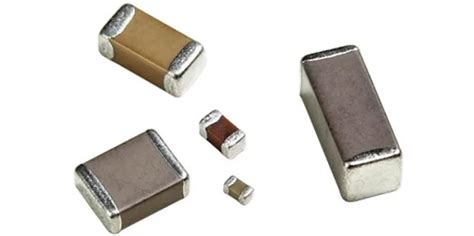
What are Surface Mount Devices (SMDs)?
Surface Mount Devices (SMDs) are the electronic components that are specifically designed for use in SMT assembly. They are attached directly to the surface of a PCB, rather than being inserted through holes like through-hole components.
SMDs come in a wide variety of packages, each designed for specific applications and manufacturing processes. Some common SMD packages include:
- Resistors and Capacitors: Chip components, MELF (Metal Electrode Leadless Face)
- Integrated Circuits: Small Outline Package (SOP), Quad Flat Package (QFP), Ball Grid Array (BGA)
- Transistors and Diodes: SOT (Small Outline Transistor), TSOP (Thin Small Outline Package)
Advantages of SMDs
- Smaller size compared to through-hole components
- Suitable for automated placement in high-volume manufacturing
- Lower lead inductance and smaller parasitic capacitance
- Better high-frequency performance
- Lower cost for high-volume production
SMD Sizing and Packaging
SMDs are usually categorized by their size and lead pitch (the distance between the leads). Two common sizing systems are the Imperial (in inches) and Metric systems.
For example, “1206” in the Imperial system indicates a component measuring 0.12 inches by 0.06 inches. In the Metric system, the same component would be labeled “3216”, indicating dimensions of 3.2mm by 1.6mm.
| Imperial | Metric | Dimensions (mm) |
|---|---|---|
| 01005 | 0402 | 0.4 x 0.2 |
| 0201 | 0603 | 0.6 x 0.3 |
| 0402 | 1005 | 1.0 x 0.5 |
| 0603 | 1608 | 1.6 x 0.8 |
| 0805 | 2012 | 2.0 x 1.25 |
| 1206 | 3216 | 3.2 x 1.6 |
| 1210 | 3225 | 3.2 x 2.5 |
SMDs are packaged for automated assembly in various ways, including:
- Tape and Reel: Components are placed in pockets on a carrier tape, which is wound onto a reel.
- Matrix Trays: Components are placed in pockets in a rectangular tray.
- Tubes: Cylindrical containers with components stacked end-to-end.
The packaging method depends on the component type, size, and the requirements of the pick-and-place equipment used in assembly.

SMT vs SMD: What’s the Difference?
While SMT and SMD are closely related terms, they refer to different things:
- SMT (Surface Mount Technology) is the method or process of assembling electronic circuits where components are mounted directly onto the PCB surface.
- SMD (Surface Mount Device) refers to the actual components that are designed for use in SMT assembly.
So SMT describes the overall technology and processes, while SMD refers to the specific components used in that technology.

Challenges in SMT Assembly
While SMT has many advantages, it also presents some challenges:
-
Miniaturization: As components get smaller, they become more difficult to place accurately and inspect. This requires high-precision equipment and rigorous process control.
-
Thermal Management: With higher component density, heat dissipation becomes a bigger issue. Careful PCB design and heat sinking are needed.
-
Solder Joint Defects: SMT can be prone to specific solder joint defects like tombstoning (where a component stands up on one end), bridging (unintended solder connections), and voiding (gaps in the solder joint). Careful process control is needed to avoid these.
-
Electrostatic Discharge (ESD): Many SMDs are sensitive to ESD. Proper ESD protection measures must be in place during handling and assembly.
-
Rework and Repair: Removing and replacing SMDs can be tricky, especially with fine-pitch components. Specialized tools and skills are needed.
Despite these challenges, the benefits of SMT – smaller, lighter, faster, and cheaper electronics – have made it the dominant technology in PCB Assembly today.

The Future of SMT
As electronic devices continue to get smaller, more complex, and more powerful, SMT will continue to evolve to keep pace. Some trends and developments to watch include:
-
Advanced Packaging: New SMD packages like Chip Scale Packages (CSP) and Wafer Level Packages (WLP) will allow even smaller and denser PCB assemblies.
-
Flexible and Stretchable Electronics: SMT is being adapted for use on flexible and even stretchable substrates, opening up new possibilities for wearables and other applications.
-
3D Printed Electronics: The integration of SMT with 3D printing technologies could allow the creation of complex, three-dimensional electronic structures.
-
Increased Automation: Advances in robotics, machine vision, and AI will drive even greater levels of automation in SMT assembly, improving speed, accuracy, and flexibility.
As these and other innovations come to fruition, SMT will remain at the heart of electronics manufacturing, enabling the creation of the ever more sophisticated devices that shape our world.
Frequently Asked Questions (FAQ)
-
Q: Can SMDs be used with through-hole technology?
A: While SMDs are designed for SMT, some can be adapted for through-hole mounting by adding leads. However, this negates many of the benefits of SMDs. -
Q: What’s the smallest SMD component?
A: Currently, the smallest commercially available SMD is the 01005 package (0.4mm x 0.2mm). Even smaller sizes are being developed. -
Q: What’s the most common cause of SMT defects?
A: Solder paste printing issues (too much, too little, or misaligned paste) are the most common cause of SMT defects. -
Q: Can SMDs be soldered by hand?
A: Yes, SMDs can be hand soldered with the right tools and technique, but it requires practice and skill, especially with smaller components. -
Q: Are all electronic components available as SMDs?
A: The vast majority of components are available in SMD packages. However, some specialized or high-power components may only be available in through-hole versions.
No responses yet