Introduction to SMT Line
Surface Mount Technology (SMT) has revolutionized the printed circuit board (PCB) manufacturing industry since its introduction in the 1960s. The SMT line is an essential part of the PCB assembly process, allowing for the precise placement of electronic components onto the surface of a PCB. This technology has greatly improved the efficiency, reliability, and cost-effectiveness of PCB manufacturing, making it the preferred method for producing high-quality electronic devices.
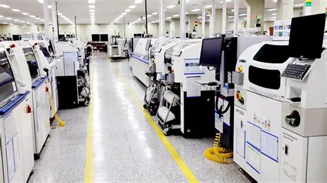
What is an SMT Line?
An SMT line is a series of machines and processes that work together to assemble electronic components onto a PCB. The line typically consists of the following equipment:
- Solder Paste Printer
- Pick and Place Machine
- Reflow Oven
- Inspection Station
Each machine plays a crucial role in the SMT assembly process, ensuring that the components are accurately placed and securely attached to the PCB.
Advantages of SMT Line
The SMT line offers numerous advantages over traditional through-hole technology (THT) in PCB manufacturing:
- Increased Density: SMT allows for the placement of smaller components, enabling higher component density on the PCB.
- Improved Reliability: SMT components have shorter leads, reducing the risk of bent or broken leads during assembly and handling.
- Faster Assembly: SMT lines are highly automated, allowing for faster placement of components compared to manual THT assembly.
- Cost-Effectiveness: The increased efficiency and automation of SMT lines result in lower production costs, making it an economical choice for high-volume manufacturing.
Key Components of an SMT Line
Solder Paste Printer
The solder paste printer is the first machine in the SMT line. It applies a precise amount of solder paste onto the PCB’s contact pads using a stencil. The stencil is a thin metal sheet with apertures that correspond to the location of the contact pads on the PCB. The solder paste is pushed through the apertures, depositing it onto the pads.
Solder Paste
Solder paste is a mixture of tiny solder particles suspended in a flux medium. The solder particles are typically made of a tin-lead or lead-free alloy, depending on the application and regulatory requirements. The flux helps to remove oxides from the metal surfaces, ensuring a strong and reliable solder joint.
Stencil Design
The stencil design is critical for achieving the correct solder paste deposit on the PCB. Factors such as aperture size, shape, and thickness must be carefully considered to ensure optimal paste release and avoid defects like bridging or insufficient solder.
Pick and Place Machine
The pick and place machine is responsible for placing the electronic components onto the solder paste-covered contact pads on the PCB. Modern pick and place machines are highly automated and can place thousands of components per hour with great accuracy.
Component Feeders
Component feeders supply the pick and place machine with a continuous stream of components. The feeders come in various types, such as tape and reel, tube, or tray, depending on the component packaging.
Vision System
Pick and place machines are equipped with sophisticated vision systems that ensure accurate component placement. The vision system captures images of the components and the PCB, allowing the machine to make necessary adjustments for any misalignments or rotations.
Reflow Oven
After the components are placed, the PCB enters the reflow oven, where the solder paste is heated to form permanent solder joints. The reflow process involves a carefully controlled temperature profile that gradually heats the PCB to the solder’s melting point, allowing the solder to flow and form a strong bond between the components and the contact pads.
Temperature Profile
The temperature profile is a critical aspect of the reflow process. It consists of several stages:
- Preheat: The PCB is gradually heated to activate the flux and remove any moisture.
- Soak: The temperature is maintained to ensure even heat distribution across the PCB.
- Reflow: The temperature is raised above the solder’s melting point, allowing the solder to flow and form the joints.
- Cooling: The PCB is cooled down to solidify the solder joints.
The precise control of the temperature profile is essential for achieving high-quality solder joints and preventing defects like cold joints, voids, or thermal damage to the components.
Inspection Station
After the reflow process, the PCB undergoes inspection to ensure that all components are correctly placed and soldered. The inspection station typically employs automated optical inspection (AOI) technology to detect any defects or irregularities.
Automated Optical Inspection (AOI)
AOI systems use high-resolution cameras and advanced image processing algorithms to inspect the PCB. The system compares the captured images with a reference image of a known good PCB, identifying any deviations or defects, such as misplaced components, solder bridges, or insufficient solder.
Benefits of AOI
AOI offers several benefits in the SMT line:
- Early Defect Detection: AOI catches defects early in the manufacturing process, preventing them from progressing to later stages where they may be more difficult and costly to fix.
- Increased Quality: By identifying and correcting defects, AOI helps to maintain a high level of quality in the finished products.
- Improved Efficiency: Automated inspection is faster and more consistent than manual inspection, reducing the time and labor required for quality control.

Process Flow of an SMT Line
The SMT line follows a sequential process flow to assemble the PCB:
- Solder Paste Printing: The solder paste is applied to the PCB using the solder paste printer and stencil.
- Component Placement: The pick and place machine places the electronic components onto the solder paste-covered contact pads.
- Reflow Soldering: The PCB enters the reflow oven, where the solder paste is heated to form permanent solder joints.
- Inspection: The PCB is inspected using AOI to detect any defects or irregularities.
- Rework (if necessary): If defects are found during inspection, the PCB may undergo rework to correct the issues.
- Final Assembly: After passing inspection, the PCB moves on to final assembly, where it is integrated into the finished product.
| Process Step | Description |
|---|---|
| Solder Paste Printing | Applies solder paste to PCB contact pads using a stencil |
| Component Placement | Places electronic components onto solder paste-covered pads |
| Reflow Soldering | Heats solder paste to form permanent solder joints |
| Inspection | Checks for defects using automated optical inspection (AOI) |
| Rework (if necessary) | Corrects any defects found during inspection |
| Final Assembly | Integrates the PCB into the finished product |

Challenges and Considerations in SMT Line Implementation
While SMT lines offer numerous benefits, there are also challenges and considerations to keep in mind when implementing this technology:
Component Miniaturization
As electronic devices become smaller and more compact, the components used in PCBs are also decreasing in size. This miniaturization poses challenges for SMT lines, as the machines must be capable of handling and placing these tiny components with high precision.
Solder Paste Selection
Selecting the appropriate solder paste is crucial for achieving reliable solder joints. Factors to consider include the solder alloy composition, particle size, and flux type. The solder paste must be compatible with the PCB material, component metallization, and reflow profile.
Reflow Profile Optimization
Optimizing the reflow profile is essential for ensuring the formation of high-quality solder joints. The profile must be tailored to the specific PCB design, component types, and solder paste used. Insufficient or excessive heating can lead to defects like cold joints, voids, or component damage.
Moisture Sensitivity
Some electronic components are sensitive to moisture, which can cause damage during the reflow process. Moisture-sensitive devices (MSDs) must be handled and stored properly to prevent moisture absorption. This may involve using moisture barrier bags, desiccants, and baking the components before assembly.
Electrostatic Discharge (ESD) Protection
Electronic components can be damaged by electrostatic discharge (ESD) during handling and assembly. SMT lines must implement ESD protection measures, such as grounded workstations, ESD-safe flooring, and personnel grounding devices, to minimize the risk of ESD damage.

Future Trends in SMT Line Technology
As the electronics industry continues to evolve, SMT line technology is also advancing to keep pace with the changing requirements:
Increased Automation
SMT lines are becoming increasingly automated, with the integration of robotics and artificial intelligence (AI) technologies. This automation enhances the speed, accuracy, and flexibility of the assembly process, allowing for faster changeovers and higher throughput.
Smart Factory Integration
SMT lines are being integrated into smart factory environments, where data from the machines is collected and analyzed in real-time. This data-driven approach enables predictive maintenance, process optimization, and quality control, leading to improved efficiency and reduced downtime.
Adoption of Industry 4.0 Technologies
Industry 4.0 technologies, such as the Internet of Things (IoT), big data analytics, and cloud computing, are being applied to SMT lines. These technologies enable remote monitoring, data-driven decision making, and seamless integration with other manufacturing systems.
Emphasis on Sustainability
There is a growing emphasis on sustainability in the electronics industry, and SMT lines are no exception. Manufacturers are adopting lead-free solder alloys, implementing energy-efficient processes, and focusing on reducing waste and environmental impact.
Conclusion
The SMT line has transformed the PCB manufacturing industry, offering a highly efficient and cost-effective solution for assembling electronic devices. By understanding the key components, process flow, and challenges associated with SMT lines, manufacturers can optimize their assembly processes and produce high-quality PCBs.
As technology continues to advance, SMT lines will evolve to meet the changing demands of the electronics industry. By embracing automation, smart factory integration, and sustainable practices, manufacturers can stay ahead of the curve and remain competitive in the global market.
Frequently Asked Questions (FAQ)
1. What is the difference between SMT and through-hole technology (THT)?
SMT involves placing components directly onto the surface of the PCB, while THT requires inserting component leads through holes in the PCB and soldering them on the opposite side. SMT allows for smaller components and higher density, while THT is often used for larger, heavier components or in applications requiring greater mechanical strength.
2. Can SMT lines handle both leaded and lead-free solder?
Yes, modern SMT lines can work with both leaded and lead-free solder pastes. However, the reflow profile and process parameters must be adjusted accordingly, as lead-free solder typically requires higher temperatures and longer dwell times compared to leaded solder.
3. How does the vision system in a pick and place machine work?
The vision system in a pick and place machine uses high-resolution cameras to capture images of the components and PCB. These images are processed by advanced algorithms that detect the position, orientation, and alignment of the components. The machine then uses this information to make necessary adjustments to ensure accurate placement.
4. What are some common defects that can occur in the SMT assembly process?
Common defects in SMT assembly include solder bridging (unintended connection between two or more leads), insufficient solder (weak or missing solder joints), tombstoning (one end of a component lifts off the pad), component misalignment, and solder balls (small spheres of solder that can cause short circuits).
5. How can manufacturers ensure the quality of the PCBs produced by an SMT line?
Manufacturers can ensure PCB Quality by implementing a comprehensive quality control system that includes:
- Incoming inspection of raw materials and components
- Process monitoring and control during solder paste printing, component placement, and reflow soldering
- Automated optical inspection (AOI) after the reflow process
- Functional testing of the finished PCBs
- Continuous improvement through data analysis and process optimization
By following best practices and investing in advanced technologies, manufacturers can produce high-quality PCBs consistently using SMT lines.
No responses yet